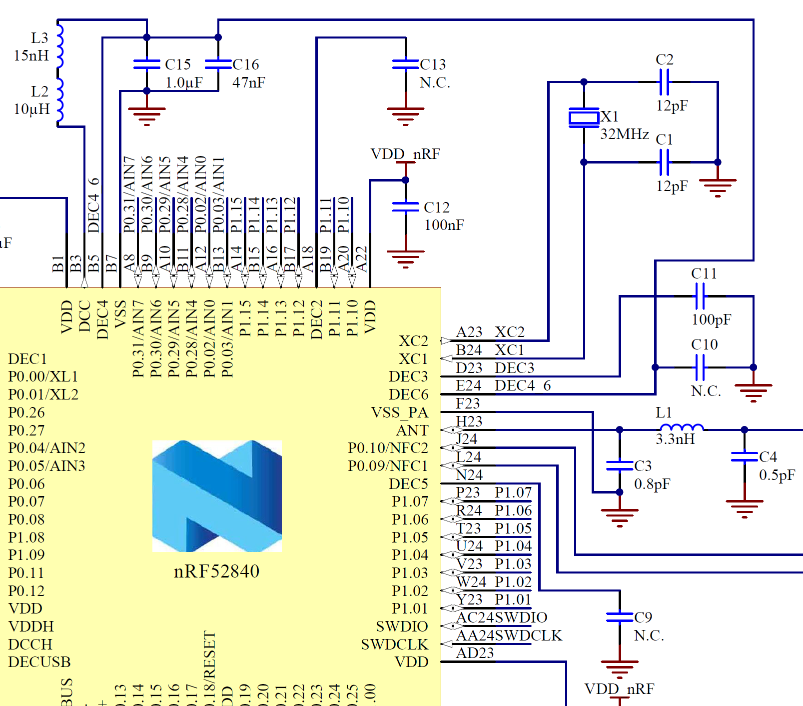
The latest Objective Spec nRF52840 Objective Product Specification v0.5.1 got me a little confused since I was working off of v0.5 until few weeks ago. My application is a cross between Circuit Configuration #5 and #6 (pg 693-694), that is, no NFC/USB/EXTSUPPLY/DCDCEN0, but yes DCDCEN1.
- In v0.5.1, pin F23 got renamed from DEC6 (in v0.5 named DEC2).
What was the nature of this change? Was it just to discern between pin A18 which is also named DEC2, did the functionality change, etc?
- In v0.5.1, pin E24 DEC6 is tied to pin B5 DEC4 with a bypass cap C16 47nF.
What was the nature of these changes? I should follow v0.5.1 in my application? Is C16 more for DEC4 than DEC6, hence adding C16 instead of C10? I assume C16 is to additionally decouple higher frequencies C15 isn't - is that the intent?
The nRF52840 preview devkit (v0.9.x) doesn’t have this change found in v0.5.1. How would this change affect results seen with the devkit?
- There are 3 capacitors (C9, C10, C13) that are in layout but not mounted (N.C.). My application is very space constrained, and I’d like to not put these in the PCB layout if reasonable.
What are these for, and how much risk would it be to the intended performance of the SoC if not putting these provisions on my PCB? The datasheet describes as decoupling for radio/flash supply but I don’t see any examples of it caps being populated.

Please advise.


