Review_4Jan.zip Hello All,
Please review the attached revised schematic and give your valuable feedback.
Please find below queries:
In case you want to know the distance of some component, then I have set the layout grid to 1mm (white dots). This can be reference for review as well to check how far or close the component is placed.
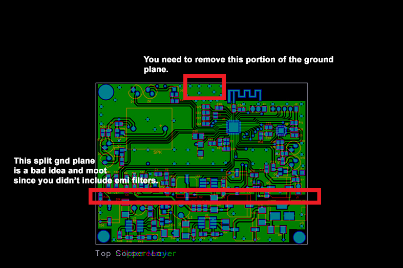
I have added copper ground layer on top and bottom. This PCB is divided into two ground parts. One is for power supply ground and other is RF and Digital ground. Both are connected at single point as shown in image Top Copper Top Silk Screen.jpg.
There is no copper layer on bottom and top side of Antenna.
IAF antenna dimensions are considered from attached reference pdf only. Please provide the correction if any especially track length from IC to LC filter and up to IAF antenna.
Attachment is password protected. password: DTA_BHS_V1.1
In schematic Programming connector is there. RESET pin is used only for programing purpose. In case programmer is not present this will be floating. So please check and correct.
Can we keep floating unused pins?
Please kindly do let’s know if you need any details in regarding this, Looking forward to hear you soon.
Thanks in advance
Pktron
Hello All.
I am working on master and multi slave project , please review my attached schematic and give your valuable feedback.
Thanks in advance pktronDTA_BHS_V1.0.pdf