
Hello,
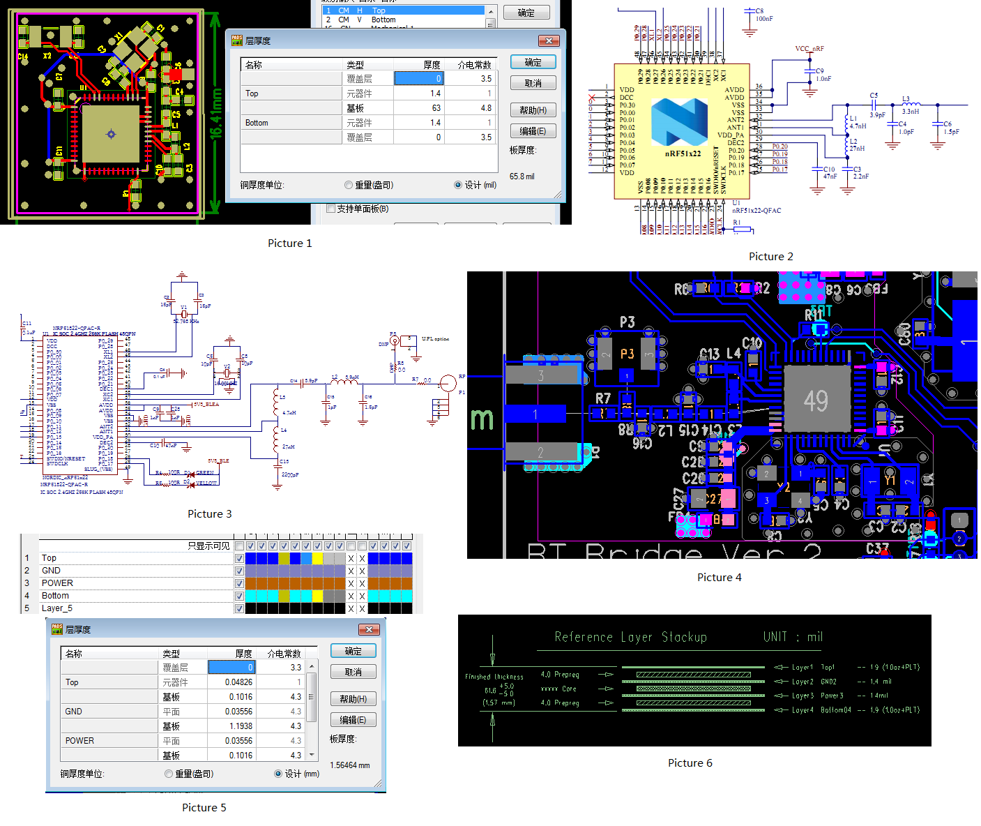
I am useing NRF51822-QFAC in my BT bridge project; Now I need to design the matching circuit; there was some recommended matching circuit in the datasheet(11.3--11.10)(Picture2 in attachment); But the reference PCB (picture1 in attachment) is just two layer with matching circuit in top layer while GND plane in bottom layer, the thickness is about 1.6mm; Now I just copy the matching circuit in my schematic(picture3 in attachment),it is not right, this matching circuit is not fit for my application,becasue My pcb(picture4 in attachment) is four layers, the layer definition is like picture 5 and picture 6 in attachment; matching circuit is in top layer, GND plane is in the second layer; the thickness between them is just about 4mils;
So I need to redesign the matching circuit, converting 15+j85 into 50 ohm; I need to convert the differential 15+j85 into a single 50 ohm; in the recommended circuit, you connected VDD_PA to ANT1 by L1 with decoupling by C3, how to concern the affect of L1 and C3 on the matching circuit? I've been checking on it for a couple of days, but can't get start...
how to design the matching circuit to match the differential 15+j*85 to 50 ohms?
picture.png
 thanks;
