This post is older than 2 years and might not be relevant anymore
More Info: Consider searching for newer posts

PCB reference Design

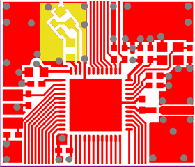
In the PCB design reference for the NRF52 we can see that the components L3 and C10 is not parallel with another components and lines. any special reason for that?

Any problem if I change this?

Also, exist two options of layout: QFAA and QFAB but  I don't found any difference in the layout.

http://infocenter.nordicsemi.com/pdf/nRF52832-QFAx_Ref_Layout_v1.1.zip

Regards

  • Hi Carlos,

    There are historical reasons for the placement of L3 and C10 as it was beneficial for testing purposes. You can change the orientation if you prefer. However, to prevent noise issues, you should place the inductors in a way to reduce the coupling between them. The big inductor should be placed close to the nRF device, and the capacitor should be well grounded.

    You are correct, the QFAA and QFAB reference layouts are identical.

    Ketil

Related