This post is older than 2 years and might not be relevant anymore
More Info: Consider searching for newer posts

RF Antenna PCB Layout Reivew

I am designing a PCB using the NRF52832 and this antenna. The antenna design guidelines suggest ground clearance and direct traces from the NRF52832 to the antenna without the use of vias. However, due to size constraints on the PCB it is difficult for me to route the antenna without vias and ground plane.


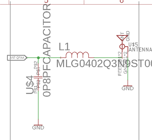
Above is the schematic I am using with a matching circuit using a 0.8pf capacitor and 3.9 nH inductor as suggested by Nordic
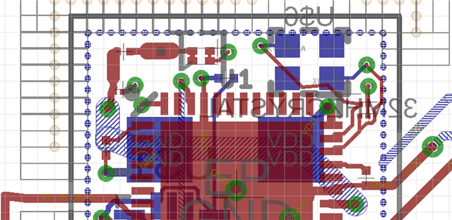
Above is a picture of the PCB layout. The blue striped trace that runs through the middle of the board is the trace from the antenna.

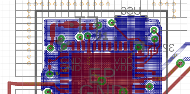
Above is a picture of the PCB layout with the ground and vcc plane.

What type of effect will the ground planes and vias have on the signal. I do not mind loss in range as I am communicating with a device only 1 - 2 meters away. What is the suggested solution for cases where clearance space is limited?

Parents
  • You can't do any of the things you have shown above.

    For starters it is required that the nRF have a ground plane and via pattern under it.  You removed it. This can not be done.

    Secondly, connecting RF on vias takes a lot of work even for RF engineers with the right tools.  Yours will not work not matter how much post effort you put into it. You asked what will be the effect of what you had shown...the effect will be as if you never even put an antenna on the board at all and just shorted out the nRF output. 

    If you want the chip and antenna to work you need to follow their design guidelines.

    I would suggest you move things around to keep the Johanson antenna on the same side as the RF output of the nRF. You will still need to provide room for the nRF output match since it is not 50ohm output.

    Another option is to switch to the WLCSP version of the nRF which is much smaller.

    And, a final option would be to run a monopole antenna along the edge of the board. But again this takes a lot of skill to design correctly.

    Here is a nice discussion on putting an antenna on a small device.  Lots of good links in it: devzone.nordicsemi.com/.../11196

Reply
  • You can't do any of the things you have shown above.

    For starters it is required that the nRF have a ground plane and via pattern under it.  You removed it. This can not be done.

    Secondly, connecting RF on vias takes a lot of work even for RF engineers with the right tools.  Yours will not work not matter how much post effort you put into it. You asked what will be the effect of what you had shown...the effect will be as if you never even put an antenna on the board at all and just shorted out the nRF output. 

    If you want the chip and antenna to work you need to follow their design guidelines.

    I would suggest you move things around to keep the Johanson antenna on the same side as the RF output of the nRF. You will still need to provide room for the nRF output match since it is not 50ohm output.

    Another option is to switch to the WLCSP version of the nRF which is much smaller.

    And, a final option would be to run a monopole antenna along the edge of the board. But again this takes a lot of skill to design correctly.

    Here is a nice discussion on putting an antenna on a small device.  Lots of good links in it: devzone.nordicsemi.com/.../11196

Children
No Data
Related