This post is older than 2 years and might not be relevant anymore
More Info: Consider searching for newer posts

Did not get "Constant carrier wave output for testing" working on nRF24L01+

Hello,

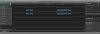
Like in the description, I dont get this to work. Im trying to get The nRF24L01+ connected to a PIC16LF18345. I did Some Pictures of the SPI logic and Here is a Part of the Code Ive written of the configuration for carrier Signal like described in the datasheet.

    while(1)
    {
    if(PORTCbits.RC4 == 0) //Startswitch
    {
    __delay_ms (2500);
        
    spi_start();
    spi_rx(0b00100000); //W + Reg CONFIG
    spi_rx(0x02); //PWR UP
    spi_stop();
    
    __delay_us(1700);
    
    spi_start();
    spi_rx(0b00100110); //W + Reg RF_SETUP
    spi_rx(0b10010110); 
    spi_stop();

    spi_start();
    spi_rx(0b00100101); //W + Reg RF_CH
    spi_rx(0x22); 
    spi_stop();

       while(1){
    PORTCbits.RC7 = 1;  //CE
                }
        }
    }

I have tried almost everything and so now im here and ask for help :) 

Parents
  • Here is some Addition Code which my help finding the Problem 

    /// HERE A PAT OF MY INTERRUPT ROUTINE 
    
    void interrupt ISR()
       {
        if (spi_Aktiv == 1)
        
        {
            if (SSP2STATbits.BF == 1)       //BUFFER FULL
            {
                SSP2IF = 0;                 //INTERRUPT FLAG
                spi_BF = 1;                 //BUFFER FULL bit für SPI.H
            }
        }

    /// HERE IS MY SPI FILE (comments in german sry:/)
    
    unsigned char spi_Aktiv = 0;    //Bit für ISR setzen bedeutet: Interrupt betrifft SPI
    unsigned char spi_BF = 0;       //Fuffer Full detection Bit
    void spi_init(){
    
    //PORT B 
        PORTBbits.RB5 = 0;
        PORTBbits.RB7 = 0;
        TRISBbits.TRISB5 = 1;       //Eingang Data In
        TRISBbits.TRISB7 = 0;       //Ausgang Clock
        ANSELBbits.ANSB5 = 0;
        ANSELBbits.ANSB7 = 0;
        LATBbits.LATB5 = 0;
        LATBbits.LATB7 = 0;
        ODCONBbits.ODCB5 = 0;
        ODCONBbits.ODCB7 = 0;
        SLRCONBbits.SLRB5 = 0;
        SLRCONBbits.SLRB7 = 0;
        INLVLBbits.INLVLB5 = 0;
        INLVLBbits.INLVLB7 = 0;
        
     //PORT C   
        PORTCbits.RC1 = 0;
        PORTCbits.RC2 = 0;
        PORTCbits.RC6 = 0;
        PORTCbits.RC7 = 0;
    
        TRISCbits.TRISC1 = 1;       //Eingang Interrupt
        TRISCbits.TRISC2 = 0;       //Ausgang Data OUT
        TRISCbits.TRISC6 = 0;       //Ausgang Slave Select
        TRISCbits.TRISC7 = 0;       //Ausgang R/W
    
        ANSELCbits.ANSC1 = 0;
        ANSELCbits.ANSC2 = 0;
        ANSELCbits.ANSC6 = 0;
        ANSELCbits.ANSC7 = 0;
    
        LATCbits.LATC1 = 0;
        LATCbits.LATC2 = 0;
        LATCbits.LATC6 = 0;
        LATCbits.LATC7 = 0;
    
        ODCONCbits.ODCC1 = 0;
        ODCONCbits.ODCC2 = 0;
        ODCONCbits.ODCC6 = 0;
        ODCONCbits.ODCC7 = 0;
    
        SLRCONCbits.SLRC1 = 0;
        SLRCONCbits.SLRC2 = 0;
        SLRCONCbits.SLRC6 = 0;
        SLRCONCbits.SLRC7 = 0;
    
        INLVLCbits.INLVLC1 = 0;
        INLVLCbits.INLVLC2 = 0;
        INLVLCbits.INLVLC6 = 0;
        INLVLCbits.INLVLC7 = 0;
    
    //PPS
    //-Input
        INTPPS = 0b00010001;  // RC1 Interrupt
        
        //SSP2CLKPPS = 0b00001110; // Clock
        SSP2DATPPS = 0b00001101; //RB5 Data
        //SSP2SSPPS = 0b00001101; //Slave Select
    //-Output
        //RB5PPS = 0b00000000; // -> LATB5 SDI2 MISO
        RB7PPS = 0b00011010; // -> SCK2
        //RC1PPS = 0b00000000; // -> LATC1 INTERRUPT
        RC2PPS = 0b00011011; // -> SDO2 MOSI
        //RC6PPS = 0b00000000; // -> !SS  SlaveSelect
        //RC7PPS = 0b00000000; // -> LATC7 NRF R/W
    //spi
        SSP2ADD = 0b11111111;  //Fosc/(4*(SSPADD[31]+1)) -> 250Kbit
        PORTCbits.RC6 = 1;      //!Slave Select deaktivieren
        SSP2STAT = 0b11000000; // CKE = 1;
        SSP2CON1 = 0b00101010; // SSPEN; CKP = 0; use SSPADD
        SSP2CON3 = 0b00000000; // Bit 4 BOEN vlt falsch
    //Interrupt
        INTCONbits.GIE = 1; //GIE + PEIE = 1
        INTCONbits.PEIE = 1;
        INTCONbits.INTEDG = 1; //Positive Flanke
        PIE0bits.IOCIE = 1; //Periperie Interrupt freischalten
        IOCCP = 0b00000010; //RC1 = interrupt mit Positiver Flanke
        SSP2IE = 1;
    }
    
    
    void spi_start(){
        spi_Aktiv = 1;          //Für interrupt
        PORTCbits.RC6 = 0;      //!Slave Select aktivieren
    }
    
    unsigned char spi_rx(unsigned char txbyte){
    
        SSP2BUF = txbyte;       //Daten in Buffer Schreiben und Übertragung starten
        while(spi_BF == 0){}    //Warten bis Buffer Voll ist (interrupt))
        spi_BF = 0;
        return SSP2BUF;         // Daten aus Buffer Lesen und in spi_rx zurückgeben
                        }
    
    void spi_stop(){
    
        spi_Aktiv = 0;
        PORTCbits.RC6 = 1;      //!Slave Select deaktivieren
        spi_BF = 0;             ////Fuffer Full detection Bit löschen
        
    }

    I have not implemented the Interrupt Routine because there was no Need for the RF carrier Signal in the PDF but if it will help i will add it just tell me.

Reply
  • Here is some Addition Code which my help finding the Problem 

    /// HERE A PAT OF MY INTERRUPT ROUTINE 
    
    void interrupt ISR()
       {
        if (spi_Aktiv == 1)
        
        {
            if (SSP2STATbits.BF == 1)       //BUFFER FULL
            {
                SSP2IF = 0;                 //INTERRUPT FLAG
                spi_BF = 1;                 //BUFFER FULL bit für SPI.H
            }
        }

    /// HERE IS MY SPI FILE (comments in german sry:/)
    
    unsigned char spi_Aktiv = 0;    //Bit für ISR setzen bedeutet: Interrupt betrifft SPI
    unsigned char spi_BF = 0;       //Fuffer Full detection Bit
    void spi_init(){
    
    //PORT B 
        PORTBbits.RB5 = 0;
        PORTBbits.RB7 = 0;
        TRISBbits.TRISB5 = 1;       //Eingang Data In
        TRISBbits.TRISB7 = 0;       //Ausgang Clock
        ANSELBbits.ANSB5 = 0;
        ANSELBbits.ANSB7 = 0;
        LATBbits.LATB5 = 0;
        LATBbits.LATB7 = 0;
        ODCONBbits.ODCB5 = 0;
        ODCONBbits.ODCB7 = 0;
        SLRCONBbits.SLRB5 = 0;
        SLRCONBbits.SLRB7 = 0;
        INLVLBbits.INLVLB5 = 0;
        INLVLBbits.INLVLB7 = 0;
        
     //PORT C   
        PORTCbits.RC1 = 0;
        PORTCbits.RC2 = 0;
        PORTCbits.RC6 = 0;
        PORTCbits.RC7 = 0;
    
        TRISCbits.TRISC1 = 1;       //Eingang Interrupt
        TRISCbits.TRISC2 = 0;       //Ausgang Data OUT
        TRISCbits.TRISC6 = 0;       //Ausgang Slave Select
        TRISCbits.TRISC7 = 0;       //Ausgang R/W
    
        ANSELCbits.ANSC1 = 0;
        ANSELCbits.ANSC2 = 0;
        ANSELCbits.ANSC6 = 0;
        ANSELCbits.ANSC7 = 0;
    
        LATCbits.LATC1 = 0;
        LATCbits.LATC2 = 0;
        LATCbits.LATC6 = 0;
        LATCbits.LATC7 = 0;
    
        ODCONCbits.ODCC1 = 0;
        ODCONCbits.ODCC2 = 0;
        ODCONCbits.ODCC6 = 0;
        ODCONCbits.ODCC7 = 0;
    
        SLRCONCbits.SLRC1 = 0;
        SLRCONCbits.SLRC2 = 0;
        SLRCONCbits.SLRC6 = 0;
        SLRCONCbits.SLRC7 = 0;
    
        INLVLCbits.INLVLC1 = 0;
        INLVLCbits.INLVLC2 = 0;
        INLVLCbits.INLVLC6 = 0;
        INLVLCbits.INLVLC7 = 0;
    
    //PPS
    //-Input
        INTPPS = 0b00010001;  // RC1 Interrupt
        
        //SSP2CLKPPS = 0b00001110; // Clock
        SSP2DATPPS = 0b00001101; //RB5 Data
        //SSP2SSPPS = 0b00001101; //Slave Select
    //-Output
        //RB5PPS = 0b00000000; // -> LATB5 SDI2 MISO
        RB7PPS = 0b00011010; // -> SCK2
        //RC1PPS = 0b00000000; // -> LATC1 INTERRUPT
        RC2PPS = 0b00011011; // -> SDO2 MOSI
        //RC6PPS = 0b00000000; // -> !SS  SlaveSelect
        //RC7PPS = 0b00000000; // -> LATC7 NRF R/W
    //spi
        SSP2ADD = 0b11111111;  //Fosc/(4*(SSPADD[31]+1)) -> 250Kbit
        PORTCbits.RC6 = 1;      //!Slave Select deaktivieren
        SSP2STAT = 0b11000000; // CKE = 1;
        SSP2CON1 = 0b00101010; // SSPEN; CKP = 0; use SSPADD
        SSP2CON3 = 0b00000000; // Bit 4 BOEN vlt falsch
    //Interrupt
        INTCONbits.GIE = 1; //GIE + PEIE = 1
        INTCONbits.PEIE = 1;
        INTCONbits.INTEDG = 1; //Positive Flanke
        PIE0bits.IOCIE = 1; //Periperie Interrupt freischalten
        IOCCP = 0b00000010; //RC1 = interrupt mit Positiver Flanke
        SSP2IE = 1;
    }
    
    
    void spi_start(){
        spi_Aktiv = 1;          //Für interrupt
        PORTCbits.RC6 = 0;      //!Slave Select aktivieren
    }
    
    unsigned char spi_rx(unsigned char txbyte){
    
        SSP2BUF = txbyte;       //Daten in Buffer Schreiben und Übertragung starten
        while(spi_BF == 0){}    //Warten bis Buffer Voll ist (interrupt))
        spi_BF = 0;
        return SSP2BUF;         // Daten aus Buffer Lesen und in spi_rx zurückgeben
                        }
    
    void spi_stop(){
    
        spi_Aktiv = 0;
        PORTCbits.RC6 = 1;      //!Slave Select deaktivieren
        spi_BF = 0;             ////Fuffer Full detection Bit löschen
        
    }

    I have not implemented the Interrupt Routine because there was no Need for the RF carrier Signal in the PDF but if it will help i will add it just tell me.

Children
Related