This post is older than 2 years and might not be relevant anymore
More Info: Consider searching for newer posts

Receiveing signal strength is jumping and different from each other of NRF52832 Gateway

hello,

Now i have two troubles in NRF52832 Gateway.

1.Planning  introduce:

  The only function of NRF52832 Gateway is to scan beacons' advertisements.  With beacons‘ number is so huge,so we use three NRF52832 chips and scanning on 37/38/39  channels respectively.But we only use one antenna(SMA footprint) in this gateway. So  rear of this antenna is a LNA chip,after LNA chip is power separator chip(1 to 3).Three NRF52832 are connected to power separator directly like image1.      
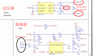
2.PCB introduce:

F2 is LNA,U4 is power separator.RF lines(green )have made 50 Ω.Like photo 2.

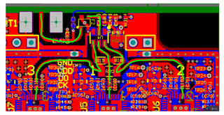
3.Our testing method.

SMA antenna is linked with a Signal generator to gerenter a 2.4GHz&2MHz bandwith ble signal.We give the signal strength is -40dBm.

NRF52832 ANT pins is linked to spectrometer to see the waveform.

4.Our finding troubles.

1. Three NRF52832 chips‘ peak point of waveform is jumping about 2dBm when  it have burned programs.After erased the program, Three peak points of waveform is stable.

2.Middle NRF52832's signal strength is better than others 4dBm.
5.My Qus:

1.I guess the reason of these two troubles is length of RF lines is so long and not equal each other.
2.How to measure to find the reason causing this two thoubles,Network analyzer?
3.My testing method is appropriate or not.

Eager to get you help.  Eager Eager...

Thanks,thanks,thanks.
liu

[email protected]

Parents
  • Hi Liu,


    This is a very uncommon application for our devices, so please understand that we have very little knowledge on this.


    Troubles:

    1. I do not understand what is jumping, transmitting or received power? Which program is burned? Which program is loaded when it is erased?

    2. The difference in signal strength is probably a combination between trace length and the middle trace just passing through 1 power divider, even though it is 3-way division. Also there should be solid ground underneath all RF paths, without ground, and with a trace passing underneath one direction, you do not have control that it will be similar.

    3. Using the RSSI module in the nRF52 is an inaccurate way to characterize this. It would be better to use a signal/spectrum analyzer. A network analyzer could be useful to see how different the loads seen by the nRF52 are.


    Best regards,

    Andreas

  • Hi,

    My PCB board is 4 layers.The second layer is GND totally.

    So,there have solid ground underneath all RF paths,and through it we made 50Ω impedance.

Reply Children
No Data
Related