I have two nrf52832 boards, both being developed with SDK v11 and the s132 soft device.
Board one is given commands over UART to communicate over ESB with board two. Board two also has serial communication with an FPGA that can be reprogrammed sucsessfully over ESB.
The goal is to be able to update the firmware on board two over ESB. Doing this will also reprogram the FPGA that currently boots from a file flashed along with the board two app via the "incbin" library.
Issues I'm having:
1. When trying to read and write to flash I discovered that DFU_BANK_1_REGION_START is in fact 0x918CB001. From my understanding this is the memory location of external RAM which is not attached and am not intending to attach. Also this not a multiple of four and is therefore not a valid boot address? The way the space for banks 0 and 1 are worked out seems to just be (BOOTLOADER_REGION_START - CODE_REGION_1_START)/2, leaves the available space around 1.75GB per bank for me, which is certainly not correct. I know i need to redefine these, but what is the best way to set the start and end position of both banks?
2. Getting the bootloader to validate the new image and swap it into bank 0 over ESB? I currently can't try this due to not being able to write into the right places in memory but any advice other than swapping over to BLE comms for bootloading or trying to change code for BLE comms with ESB protocols throughout the DFU example would be appreciated.
Thanks in advance
Jack

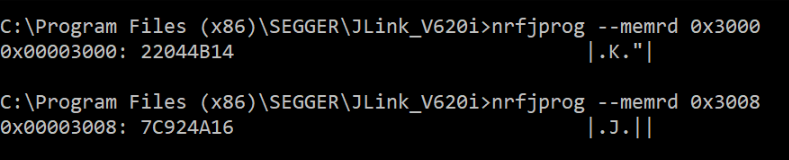
 This is what I get, soft device is s132 v2.0.0
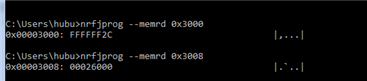
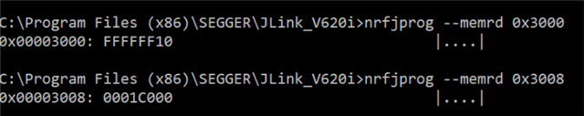