Hi
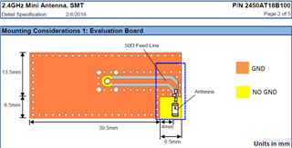
I was designing nrf52832 based PCB and using Jhonson's 2.4ghz antenna. The PCB is 2 layer and I am following the guidelines of chip antenna as given in the datasheet. The final PCB thickness would be 0.6mm so as to decrease the feed line width and to make its impedance 50ohm .
Question-
1. The matching network given for nrf52832DK kit antenna (Although, they are using trace antenna) is different from the matching network given in the chip antenna datasheet. So is it fine to go with the chip antenna matching circuit given in datasheet? (fig attached).
2. For 2 layer PCB( Top and Bottom), should the bottom layer include ground plane?
3. Is it fine to decrease board thickness to 0.6mm (becuase if there is a ground plane on the bottom layer, it may cause stray capacitance which will reduce the RF performance)?