This post is older than 2 years and might not be relevant anymore
More Info: Consider searching for newer posts

nRf51822QFAC antenna design

Hi all!

Antenna that used in nRf51822 developement kit:

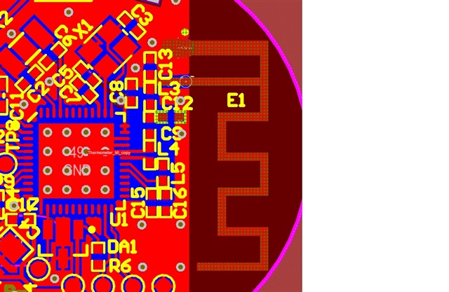
too big for my design, so I tried to use antenna that  I copied from TI AN430:

There is devices that use "the same" antenna:

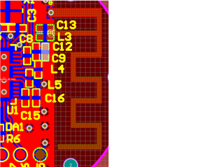
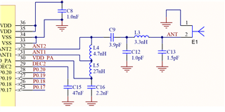
and I think  it works well. My board doesn't advertise at all. Could anyone advise me what's wrong in my board? I used Rf schematics as it is in nRf51822 Kit:


Any advices would be highly appreciated!

Parents
  • Hi,


    Even if you copied the antenna it will likely not be tuned. The extent of detuning will vary, but you should be able to see some advertising if you place it right next to your phone/DK/tester. Also your matching network layout is not ideal, as is placing the U.FL connector in parallel with the antenna, but I would still expect to see some activity if placed right next to your tester.


    Have you tried testing if your crystal starts up? Or if you are able to discover any advertising if you connect an external antenna to the U.FL connector?


    Best regards,

    Andreas

  • Hi, Andreas!

    Thank you for your answer. I have no U.FL connectors in my board. May be components C13 & L3 looks like it's the connector.  But I agree, design is not ideal. I made "Frankenshtein" - cut antenna from this board, cut antenna from board with another design that works well, glue&solder this antenna to another board. Antenna works pretty good!

    Now I've redesigned my board in a way that Nordic advise:

    Hope it will work. If you'll find something wrong, please inform

    Best Regards

    Alexander

  • Hi Alexander,


    Aha, my apologies, I confused it with the image of the module that uses the same antenna. In this case, the last layout attachment, the design looks much better. Still, you might need slight BOM changes to optimize the output power and spurious rejection of the nRF51 matching network. The antenna does not have any tuning components, so if the antenna is not perfectly tuned to 50 ohms. Both this, and the nRF matching network should be more than good enough for you to see advertisements at short range, at least when put right up against each other.


    One thing that surely will have an effect on the antenna performance is if there is anything in the bottom layer. I am not able to distinguish the color too well, but if there is copper or solder paste below, this will have a hit on performance. Solder mask opening is fine.


    Other than that I suspect the crystal not working properly, either being incorrectly tuned or not starting. What is CL and the load caps for your crystal?


    Best regards,

    Andreas

  • Hi, Andreas!

    Thanks again for your answer.

    As I understand, RF matching network is the three components - 1pF+1,5pF caps and 3,3 uH inductor near the antenna? I should change it's values using Smith's charts as it written in nWP-017 ? 

    There's nothing in bottom layer of my board. One thing that I'd like to know is how board thickness and material affect to antenna performance? I used 0,5 mm FR-4 for my board.

    Crystal works properly, I can debug any of Nordic examples (and my code) using JTAG. I used 12 pF 0402 NPO caps for crystal's loads, but what is CL?

    Best regards

    Alexander

Reply
  • Hi, Andreas!

    Thanks again for your answer.

    As I understand, RF matching network is the three components - 1pF+1,5pF caps and 3,3 uH inductor near the antenna? I should change it's values using Smith's charts as it written in nWP-017 ? 

    There's nothing in bottom layer of my board. One thing that I'd like to know is how board thickness and material affect to antenna performance? I used 0,5 mm FR-4 for my board.

    Crystal works properly, I can debug any of Nordic examples (and my code) using JTAG. I used 12 pF 0402 NPO caps for crystal's loads, but what is CL?

    Best regards

    Alexander

Children
  • Hi Alexander,


    The 1.0pF, 1.5pF and 3.3nH are a part of the nRFmatching netowrk, to tune the antenna you need other components than this, placed between the antenna and the 1.5pF. These components are then modified, based on the S-parameters you measure (smith chart).


    The board thickness should not affect this antenna too much. Yes, it will probably change the optimal tuning slightly, but it will completely destroy it.


    CL is a parameter specified for your crystal, used to determine the load capacitors (C5 and C3). You should use the formula C5 = C3 = 2*CL - 4 pF, choosing C5 and C3 far from this will cause the frequency accuracy to exceed the 40ppm requirement for Bluetooth. If exceeding this you have no guarantee that devices will be able to communicate.


    You mentioned trying to cut this (non-functional) antenna to another board, but did you try to add a replacement antenna to this (non-functional) board? You can try to just solder a wire (solid, not stranded), about 23mm long in place of where the antenna was removed. If that does not do it, you are welcome to register a private case for shipping one of your samples to us for testing.


    Best regards,

    Andreas

  • Hi Andreas!

    The problem solved. Device with last PCB design works well. Thank you for your help

    Best regards

    Alexander 

Related