This post is older than 2 years and might not be relevant anymore
More Info: Consider searching for newer posts

nrf52832 ble problem

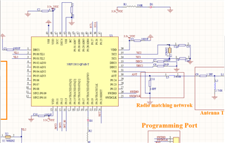
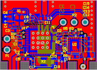
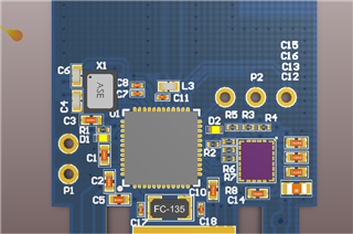
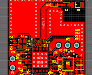
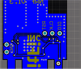
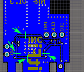
I have designed nrf52832 customized board with tace antenna antenna and every pin of the controller is connected to the male headers present on both side of the boards. I havent used lpkf , so I changed the sdkconfig.h file to use internal RC but it wasnt working. By mistake , the P0.07 pin gets connected to Vcc and the led start blinking i.e. the bluetooth is advertising. Now ble is working fine but everytime I have to connect this P0.07 with 3.3v or also with little variation on that pin (like when I Just touch that pin with my fingers). I want to kmow that P0.07 is just an I/o pin , so why this behaviour? DOes it mean there is problem in my layout design.

There is no problem in the code as I'm using the standard code of ble of nrf52 dk by changing the sdkconfig.h as we dont have lpkf

Parents
  • Ohk I will post you the schematic and layout soon. But a quick question,as you have said, the capacitor size matters!!.

     I have used various 0201 capacitors instead of 0402 and 0603 but with the same specs given in nrf datasheet. Does that honna make any difference?

  • I should have said “capacitance value”. For the logic portion of the chip, the physical size is not too important. But since the SRF ( series (or self) resonant frequency ) is strongly correlated with the value, it is best to use a combination of large and small value caps as they do in the reference design. 

    On the RF the physical size of the cap influences the size of the pads and microstrips that should be used. This is more a method of controlling parasitic reactances on RF.

    Our own designs make use of 0201 parts for much of the logic and all of the RF. Only bulk storage capacitance is made up of 0402 and 0805s. We utilize 0805s since our main product is a coin cell powered device. Thus we need a lot of local capacitance.

    happy to review your design and provide feedback.

  • Hi, Please find the below attachment. I would really appreciate if you can sort out the issue.

    In conclusion, we have to short any pin( P0.07 to P0.10) with 3.3v , and then nrf start advertising ,not without that. SO please check the attachments and let me know where we are doing wrong.

    Also, as you have mentioned that your product is cell based, and for that you are using 0805 package. In our case, we are also going to give power through button cell ( but now, we are just powering it through constant 3v supply from another board), so please explain me properly the significance of 0805 in this case.

    I would really appreciate.

  • Please post the ground plane layer too.

    On your question regarding the 0805 caps, coin cell batteries have very poor current sourcing capabilities. In my lab, I simulate them by putting 200ohms in series with the bench supply.

    I talk about it a lot on this site.  You should read the Texas Instruments white paper on the subject and also look at a coin cell spec.

    Using a coin cell and no external current consuming circuitry, the best you can expect is about 2% duty cycle assuming you put about 22uF of MLC caps on the board. Thus why I use 0805 parts.  Our design actually has an external PA uses much more power.  So we place about 100uF of MLC caps. 2x 47uF 0805 and 2x 2.2uF 0402.

    Here are some recent devzone comments on it: https://devzone.nordicsemi.com/search?q=ambystomalabs%20ti%20coin%20cell

Reply
  • Please post the ground plane layer too.

    On your question regarding the 0805 caps, coin cell batteries have very poor current sourcing capabilities. In my lab, I simulate them by putting 200ohms in series with the bench supply.

    I talk about it a lot on this site.  You should read the Texas Instruments white paper on the subject and also look at a coin cell spec.

    Using a coin cell and no external current consuming circuitry, the best you can expect is about 2% duty cycle assuming you put about 22uF of MLC caps on the board. Thus why I use 0805 parts.  Our design actually has an external PA uses much more power.  So we place about 100uF of MLC caps. 2x 47uF 0805 and 2x 2.2uF 0402.

    Here are some recent devzone comments on it: https://devzone.nordicsemi.com/search?q=ambystomalabs%20ti%20coin%20cell

Children
  • Thanku so much, I will go through the above link. and please find the following attachments-

  • Well broken ground plane seems to be your problem.

    As I show in the following image you have essentially isolated the ground of the nRF from the rest of the circuitry.  This is very, very bad.  It looks like the nRF might have a sliver of a ground connection at C7, C8 but even that is marginal.

    The way you have done the layout on your board none of the local capacitances are really doing anything since they are not connect to the same ground as the nRF.

    As to why it works when you hook up the gpio, some level of physics magic is happening.  Perhaps you are stabilizing the ground reference with that connection.

    For starters to prove to yourself that is the problem, solder some 30 gauge wires across your broken bottom layer in a few places and the problem should go away.  But you are going to have to redo your layout to fix it.

    I recommend you pass your updated layout by me for review when it is ready.

    Bridge the ground like this and see if it starts working.  Just scratch off some of the solder mask to connect the wires. Use really small gauge hookup wire, like 30 or 32 even 40 gauge is fine. On the Vss connection at pin 45 you can probably bridge it with a little dab of solder.  Just be careful not to short the pins.  If this connection scares you, then do the others first and see how it goes.

  • You don't have to do the connections precisely as I have shown, but you need at least 4 good connections around the chip to solve the problem and more connections is better.

Related