This post is older than 2 years and might not be relevant anymore
More Info: Consider searching for newer posts

SPI connection between nrf52832 and Raspberry 3 Pi

Hello guys,

I'm having problems with communication between a dwm1001 module (from Decawave) which is a nrf52832 board, and my Raspberry 3 Pi model B.

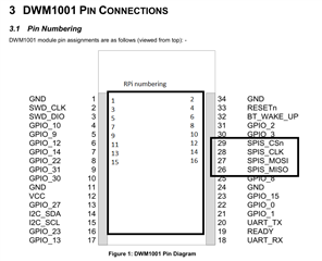
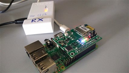
I have connected the nrf52832 board to the Raspberry using the 26-pins header

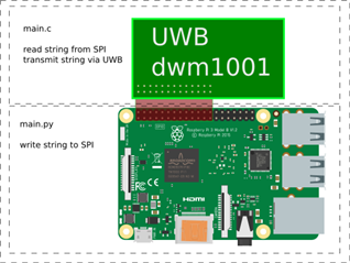
My goal is to send/write a message from Raspberry to dwm1001 module. Inside the Raspberry I wrote a simple python script in order to write to the SPI port:

import spidev
import time
spi = spidev.SpiDev()
spi.open(0,0)
spi.mode = 0b00
while True:
    data = [ 0xcc ]
    resp = spi.xfer(data)
    print resp
    time.sleep(1)

So, now I don't know if this *is* the correct way, but I have found this in internet.

In the other side, that is the nrf52832 board, I currently implemented the C code firmware so read from SPI.

#define SPI_INSTANCE  0 /**< SPI instance index. */
static const nrf_drv_spi_t spi = NRF_DRV_SPI_INSTANCE(SPI_INSTANCE);  /**< SPI instance. */
static volatile bool spi_xfer_done;  /**< Flag used to indicate that SPI instance completed the transfer. */

#define TEST_STRING "Nordic"
static uint8_t       m_tx_buf[] = TEST_STRING;           /**< TX buffer. */
static uint8_t       m_rx_buf[sizeof(TEST_STRING) + 1];    /**< RX buffer. */
static const uint8_t m_length = sizeof(m_tx_buf);        /**< Transfer length. */

/**
 * @brief SPI user event handler.
 * @param event
 */
void spi_event_handler(nrf_drv_spi_evt_t const * p_event,
                       void *                    p_context)
{
    spi_xfer_done = true;
    NRF_LOG_INFO("Transfer completed.");
    if (m_rx_buf[0] != 0)
    {
        NRF_LOG_INFO(" Received:");
        NRF_LOG_HEXDUMP_INFO(m_rx_buf, strlen((const char *)m_rx_buf));
    }
}

int main(void)
{
    bsp_board_leds_init();

    NRF_LOG_INIT(NULL);
    NRF_LOG_DEFAULT_BACKENDS_INIT();

    NRF_LOG_INFO("SPI example.");

    /*
    FROM Decawave
    
    #define SPIS_MISO_PIN   28  // SPI MISO signal.
    #define SPIS_CSN_PIN    12  // SPI CSN signal.
    #define SPIS_MOSI_PIN   25  // SPI MOSI signal.
    #define SPIS_SCK_PIN    29  // SPI SCK signal.

    #define SPIM0_SCK_PIN   2   // SPI clock GPIO pin number.
    #define SPIM0_MOSI_PIN  3   // SPI Master Out Slave In GPIO pin number.
    #define SPIM0_MISO_PIN  4   // SPI Master In Slave Out GPIO pin number.
    #define SPIM0_SS_PIN    5   // SPI Slave Select GPIO pin number.

    #define SPIM1_SCK_PIN   16  // DWM1001 SPIM1 sck connected to DW1000
    #define SPIM1_MOSI_PIN  20  // DWM1001 SPIM1 mosi connected to DW1000
    #define SPIM1_MISO_PIN  18  // DWM1001 SPIM1 miso connected to DW1000
    #define SPIM1_IRQ_PRIORITY APP_IRQ_PRIORITY_LOW // 
    #define SPIM1_SS_PIN    XX  //  Not used with DMW1001

    #define SPIM2_SCK_PIN   12  // SPI clock GPIO pin number.
    #define SPIM2_MOSI_PIN  13  // SPI Master Out Slave In GPIO pin number.
    #define SPIM2_MISO_PIN  14  // SPI Master In Slave Out GPIO pin number.
    #define SPIM2_SS_PIN    15  // SPI Slave Select GPIO pin number.
    */

    nrf_drv_spi_config_t spi_config; //= NRF_DRV_SPI_DEFAULT_CONFIG;
    spi_config.ss_pin    = NRF_DRV_SPI_PIN_NOT_USED; //SPI_SS_PIN;
    spi_config.miso_pin	= 18; //SPI_MISO_PIN;
    spi_config.mosi_pin	= 20; //SPI_MOSI_PIN;
    spi_config.sck_pin  = 16; //SPI_SCK_PIN;
    spi_config.orc		= 0xFF;
    spi_config.frequency = NRF_DRV_SPI_FREQ_125K;
    spi_config.mode      = NRF_DRV_SPI_MODE_1;
    spi_config.bit_order = NRF_DRV_SPI_BIT_ORDER_MSB_FIRST;
    nrf_drv_spi_init(&spi, &spi_config, spi_event_handler, NULL);

    while (1)
    {
        // Reset rx buffer and transfer done flag
        memset(m_rx_buf, 0, m_length);
        spi_xfer_done = false;

        
        ret_code_t ret = nrf_drv_spi_transfer(&spi, m_tx_buf, m_length, m_rx_buf, m_length);
        NRF_LOG_INFO(" Code: %d:", ret);

        while (!spi_xfer_done)
        {
            __WFE();
        }

        NRF_LOG_FLUSH();

        bsp_board_led_invert(BSP_BOARD_LED_0);
        nrf_delay_ms(200);
    }
}

But I cannot read anything. In practice I checked that the flow passes through the spi_event_handler function, but my goal is not reached.

Finally, my very final goal is the following:

Thanks in advance.

  • At that point, I'd suggest tracing what's going on on the pins. Do you have a scope or a logic analyzer?

    Also, I would find it surprising if your RPi pin 12 ("#define PIN RPI_GPIO_P1_12") would be connected to nRF PIN12 ("spis_config.csn_pin = 12;") - strange coincidence at least, but I know nothing about the board you're using (dwm1001?), maybe it is designed to resemble RPi pinout?

  • Yes, you are right.

    I made a mistake because I read the several #define online and not in the dwm1001 documentation.

    And the updated code:

        nrf_drv_spis_config_t spis_config = NRF_DRV_SPIS_DEFAULT_CONFIG;
        spis_config.csn_pin               = 29; //12; //APP_SPIS_CS_PIN;
        spis_config.miso_pin              = 26; //28; //APP_SPIS_MISO_PIN;
        spis_config.mosi_pin              = 27; //25; //APP_SPIS_MOSI_PIN;
        spis_config.sck_pin               = 28; //29; //APP_SPIS_SCK_PIN;

    I did not use wires but the 2x13 pins header. So I connected the pins 1-26 (RPi) and 1-13;22-34 (dwm).

    But still doesn't work.

    About your question about logic analyzer... I don't have anything :(

  • Unfortunately, it's little more complicated. You need to chase the pin connections through all the docs, as the only numbering that matters to your nRF code is the GPIO numbering of the nRF52832 chip inside the DWM1001 module soldered on DWM1001-DEV board connected on top of the RPi.

    I tried tracing it through all the docs and this is what I found (which could be wrong):

    Signal labelled SPIS_CSn (brought to the RPi position 24, which is GPIO8) is routed to the module castellation slot 29, which is internally routed to nRF chip pin P0.3

    SPIS_CLK is on RPi position 23 (GPIO11), slot 28, chip pin P0.4

    SPIS_MOSI is on RPi position 19 (GPIO10), slot 27, chip pin P0.6

    SPIS_MISO is on RPi position 21 (GPIO9), slot 26, chip pin P0.7

        spis_config.csn_pin               = 3; // GPIO8/SPI_CE0 on RPi
        spis_config.miso_pin              = 7; // GPIO9/SPI_MISO on RPi
        spis_config.mosi_pin              = 6; // GPIO10/SPI_MOSI on RPi
        spis_config.sck_pin               = 4; // GPIO11/SPI_SCLK on RPi 

    If you don't have a scope, you could at least try verifying individual pins (one by one), for example with a testing firmware that would just toggle each tested pin at 1Hz, so you could see if that's the one usin LED or a multimeter.

  • Hello again.

    Yesterday I tried first to set the correct pins (3, 7, 6, 4) without success.

    Second, I merged the simple SPI slave code into my "main" firmware obtaining a big and I think an unresolvable problem: the regular examples provided by DWM1001 use the SPI master.
    In other words, I'm having some troubles during compilation of my firmware since I need to include "spi slave" but dwmboard already includes "spi master".

    I suppose that both spi slave and master cannot coexist. 

    Maybe I have to change the strategy in order to communicate between raspberry and dwm1001-dev board. For strategy I mean to exploit USB, I2C, BLE, and so on...

  • SPI master and SPI slave can both be used.

    nRF52832 has 3 SPI instance, each of them could be used independently as either SPI master, slave or even TWI.

    So while the DWM module uses SPI to talk to the other chip on the module, you can still use other instance.

    In the code you have posted before, you use "#define SPIS_INSTANCE 1". You may try also using 0 or 2 (I don't know which one is used by the DWM internally).

    See the Table 6 in Chapter 8.4 on page 21 of the nRF52832 Product Specification.

Related