Hello,
I am trying to fabricate a board based on the Thingy design, including the accelerometer.
I positioned the components, traces, vias and pads following some recommendations found in this forum, used the same components found in the Thingy BOM and I will do the assembly by hand because I need to have it working ASAP.
Following is the link of my board: easyeda.com/editor shape is because I need to match the space available in the housing…I have these questions:
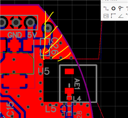
1. I added more vias to have more contact between the ground planes (following one recommendation), I tried to do it locating them in the empty space of my board. Are they correctly positioned?
2. However, in Altium I see that the vias are 0.305 mm and my local PCB manufacturer only handles vias minimum of 0.4 mm…could this be a problem for the performance of the ground planes?
3. In the Thingy design the antenna is in the border of the PCB, and at least on two sides there are no components. In my design I had to put part of the ground plane close to one of the antenna sides, leaving only one side with nothing around. Do you think this could cause a problem?
I sincerely appreciate if you see something that I am not taking into consideration on the design.