This post is older than 2 years and might not be relevant anymore
More Info: Consider searching for newer posts

nRF52840 BLE doesnt work

Hello,

we developed our electronics with your chip nRF52840, but we have problem with communication throught BLE. We tried our firmware on dev kit with this chip. It was ok. After that we developed our board. Inspired with a n RF52840 dev kit, but with a chip antenna 2450AT18B100. It works but, badly. New revision of our boards can not be find, if we use BLE scanner in our phones for detect our board. Probably our matching circuit on board is bad.
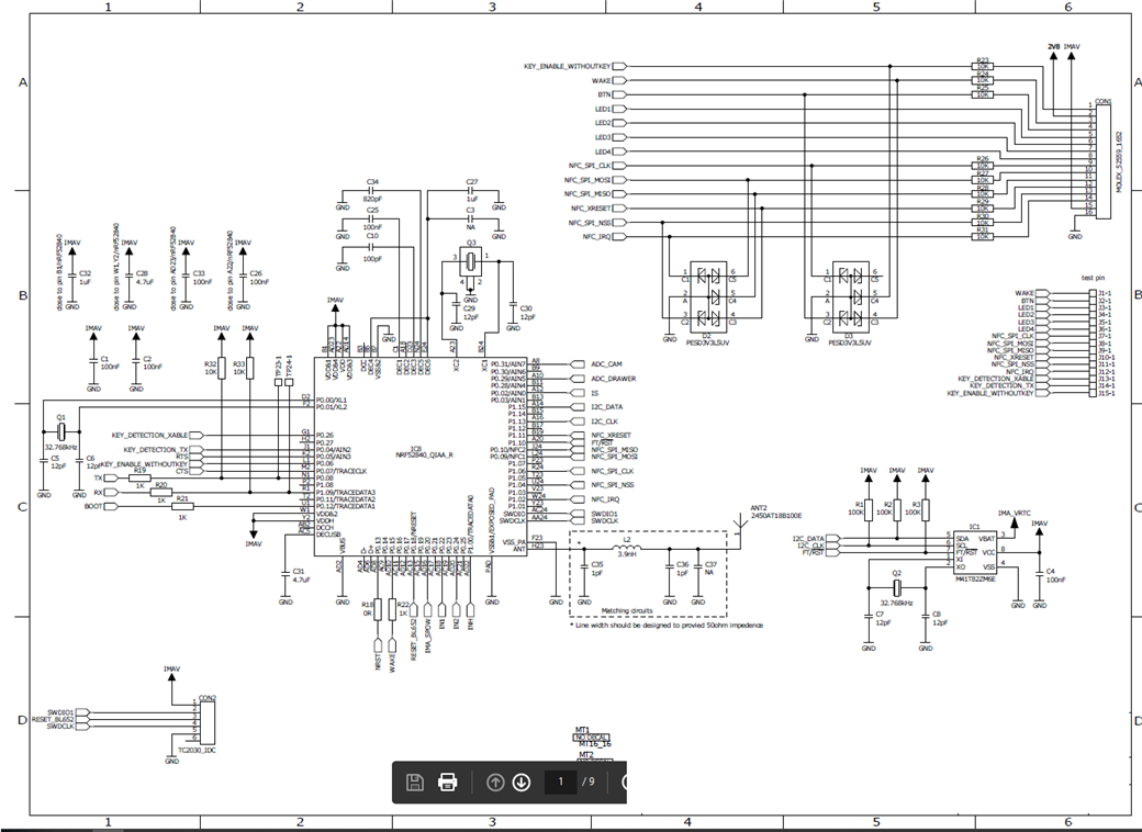
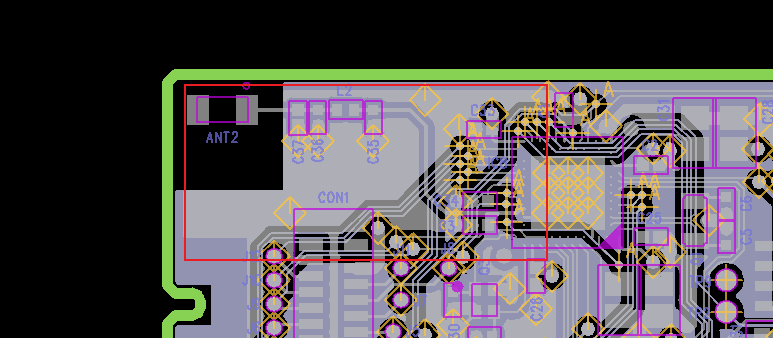
BLE part schematicsPCB part BLE layers TOP and BOTTOM) (IN2 Ground, IN3 supply)

Next our step was unsolder chip antenna and on their place try solder a thin long wire and cut that wire mm by mm. Still doesn‘t work. The devices can not be find in our BLE scanners. We tried unsolder capacitance from our matching circuits from desks and later all matching circuit on pcb. Inductor was raplaced by short. Same result.

So. We have firmware and we know: it‘s ok. Our hardware doesn‘t work in RF part. What we can change, try for get better result?

We need find a solution for the already made boards.

Parents
  • What's the CL value of the crystal? You're using 12 pF caps, which indicates a CL value of 8 pF. The formula is Ccap = CL * 2 - 4 pF. With the wring cap value, the radio will be out of spec.

    It's hard to see on the layout as the layers are stacked, but it looks like you are using only 2 layers. If so, you can not have any tracks crossing the RF section. The bottom side should be as solid as possible. Alternatively, use an inner layer as ground.

    Use plenty of vias, at least one every 10 mm in both x and y direction to connect the two ground planes firmly together.

    The matching network for the radio must be placed according to the reference layout, close to the radio. You need separate tuning components for the antenna, see this whitepaper. 


  • The CL value of crystal is 6 pF.

    Our PCB has 4 layrs. The inner layer unter top layer is GND, third layer is supply voltage.

    Ok, if we will make new pcb, we will respect this paper. Now, but we need get our existing electronics to working state. It's any chance? What we can do now?

    If we wil use antenna chip 2450AT18B100… Does we have to use matching circuit  from this document https://www.johansontechnology.com/datasheets/antennas/2450AT18B100.pdf? (matching circuit for nRF+ matching circuit for antenna)?


  • For a 6 pF crystal, you need 8.2 pF load caps. Try changing those first and see if you can get the link up. The range can be shorter than optimal, but you should be able yo get a link with a few meters of range. 

    The antenna datasheet describes one possible matching circuit, you can use this one or the PI-network described in the whitepaper. 

  • Hello,
    thank you, we tried change caps with caps 8.2 pF, but failed again. After that we changed crystal with capacitors from old board. We received advertise from the   nrf52. We had bad crystal. Range is shorter and some mobile phones(Huawei) can not connect. Probably it is bad impadance maching circuit from the antenna.

Reply Children
Related