This post is older than 2 years and might not be relevant anymore
More Info: Consider searching for newer posts
This discussion has been locked.
You can no longer post new replies to this discussion. If you have a question you can start a new discussion

JLinkExe: can not connect to target (nRF51822 - G0 rev)

Hi all !

I have been working on an nRF51822 based board for a little while, the ten 1st prototypes worked well so we asked our factory to make 20 other with the same design files.

Even after a hard week of debugging (and PAN doc + forum investigation), we still struggle to find why we get can not connect to target.

The CPU revision is now a G0 and the 1st batch had a C0 but it should not be a problem. Anyway, to demonstrate this problem, we made a couple of videos / pictures to compare the faulty batch to the old one, which works.

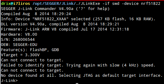
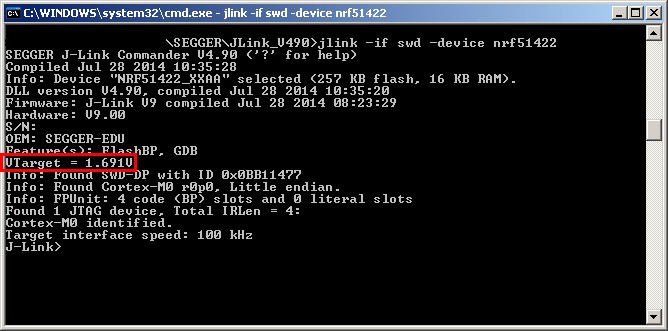
  1. We connect the probe and launch JLinkExe -if SWD -device nRF51822 to see if the CPU is detected, but it works on the old boards, not on the new one:

http://youtu.be/y9m2hepluYI

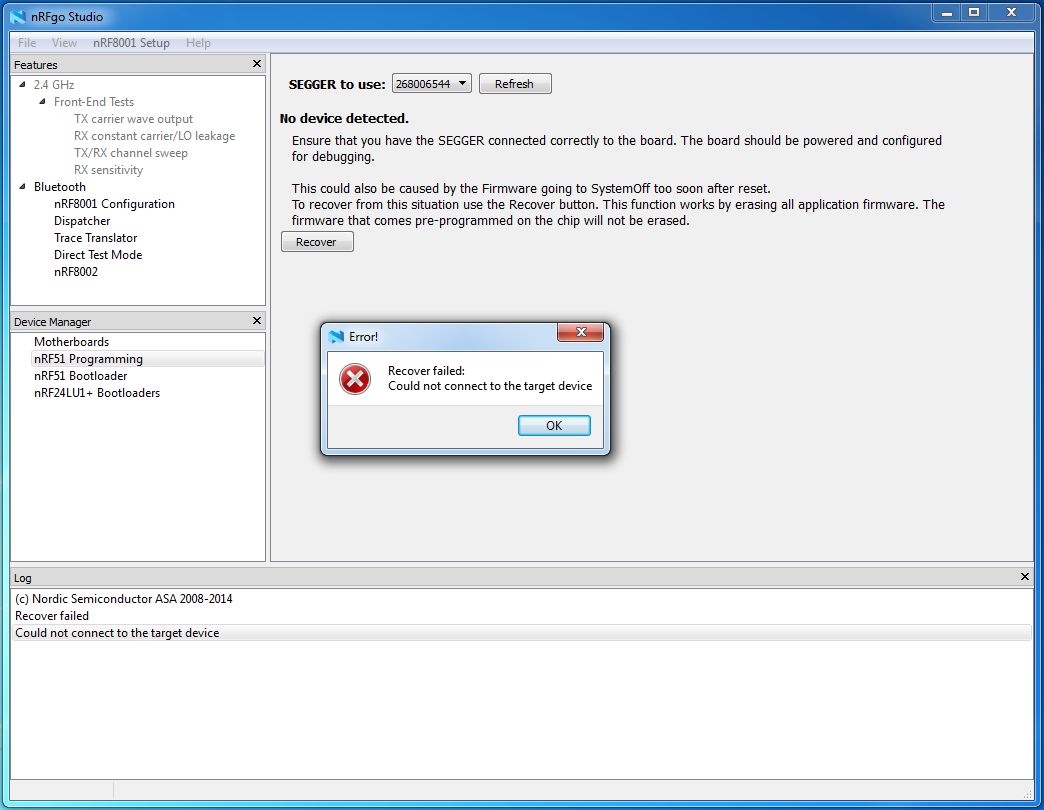
  1. We also tried to recover the CPU with nRF go studio but it failed too:

image description

  1. The power supply could be a problem so we checked it and we compared all the decoupling capacitors, no problem there.

EDIT: we also tried to power the board with 3.3V but it didn't help (thanks a lot Nguyen Hoan Hoang for the suggestion):

image description

There is a difference in the DEC1 pin voltage between C0 and G0 revisions though, but we compared with another working G0 board and it's coherent:

http://youtu.be/3gECKF1CVys

  1. The PCBs are beautiful and cleanly soldered so we don't think that it can be the problem, but we might be wrong.

EDIT2: We've also investigated the way the reset is done but we didn't find much that could help. Is it possible without a jlink connection ?

Would anyone have any suggestion on further investigations to understand what's wrong with these boards ?

Thanks a lot for your help !

Cedric ;)

PS: if the design can be helpful, it's open source and available online: portfolio.honnet.eu/twi

  • So you really confirm that if a GPIO is stuck to another one or to GNC/VCC, the probe might not be able to reset/flash the CPU ?

    Wouldn't it be a very strange coincidence if all the 2nd batch boards had bad PCB / solder mask ? (their 1st batch was good and I didn't change the design)

    I don't have the tools to unsolder the CPU so I guess I'll have to try with a pan. Would you have another trick to suggest ?

    Thanks again and again !!

    Cedric ;)

  • Do you have a meeter that can beep on conductivity ? check the pcb trace if it reaches the pin. It could be a problem with the crystal too. Verify the crystal and the 2 capacitors. I am running out of ideas too :)

  • Haha, you've been giving a lot of awesome ideas, that's just amazing... Do the CPU really need a crystal to be programmed by a Jlink probe ? (I didn't think) I'll publish the results as soon as I'll have checked all your suggestions ;) Thanks thanks thanks !!

  • Target voltage down to 1,7V shouldn't be a problem in QFN48 with internal LDO regulator connection, using j-link EDU, hw 9.0. Also flashing of nRF51422 rev. E0 works at 1,7V (less than minimum operating voltage 1,8V!)

    image description(/attachment/6a0f2f2fdb11b36a572fa420990e4e8a)

  • Try to check for short circuit between DEC1 and GND. DEC1 voltage should be 1.2V. I don't know how can another G0 device work with 0V on DEC1:

    but we compared with another working G0 board and it's coherent

    Also check DEC2 voltage.

Related