
The subject really says it all; why are there four GPIOs tied to P0.18 which is the nRF52840's RESET# pin?
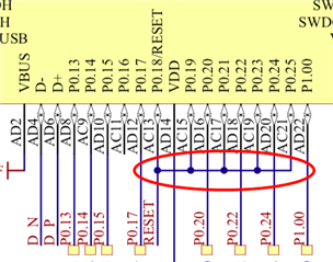
I'm looking at the PCA10059 Schematic available in the nRF52840 USB Dongle - Hardware Files 1.0.0 zip file.
The subject really says it all; why are there four GPIOs tied to P0.18 which is the nRF52840's RESET# pin?
I'm looking at the PCA10059 Schematic available in the nRF52840 USB Dongle - Hardware Files 1.0.0 zip file.
