This post is older than 2 years and might not be relevant anymore
More Info: Consider searching for newer posts

Some doubts about nrf24ap2 hardware reference circuit.

Hi Great Nordic Team: 

I have some questions about nrf24ap2 reference schematic, please kindly help to give me some tips.

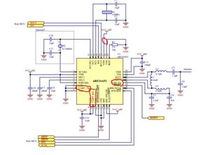
※it's reference circuit of Synchronous (bit) mode schematic of 24AP2

1. Cause VDD_PA and ANT_1 are connected though an inductor L2, will the VDD_PA  power reverse back into ANT1,and makes damages to it?

2. Why does reference circuit made the unused UART_TX and UART_RX pins  connected to different level(GND/VDD)?  Will it cause bad effect if we connect both UART_TX and UART_RX to GND ?

3. Does Pin 27 VDD needs a Coupling capacitor for noise reduction?

4. If we'd like to share RF antenna with a GPS module by diplexer (885060), will it make a impact to performance of 24AP2 ??


Thanks for your great patient. Any suggestion will be great!

Parents
  • 1. VDD_PA is the power supply to the PA. There must be a DC path between this pin and both ANT pins. Hence the inductors L1 and L2. 

    2. In synchronous mode, UART_TX and UART_RX should be tied to GND or VDD, see the the pin function, chapter 2.4 and Host interface, chaper 5 in the datasheet.

    3. All necessary decoupling capacitors are shown in the schematic.

    4. The GPS uses a different frequency, 1575 MHz, so unless you find a antenna that covers both band, it's not possible. In any case, the attenuation in a diplexer isn't good enough to allow for GPS receiving when the AP2 is transmitting. The GPS sensitivity is very high so it's not easy to share the antenna with anything else. 

  • Hi Ketiljo:

    Item 4:

    If we want to use a diplexer, how about that attenuation require?

    Could you help check two part as below which one you suggest? Or you have recommend part?

    EPCOS: B39162B8636P810

    TDK: DPX205850DT-4052B3

    Thanks a lot!

Reply Children
No Data
Related