This post is older than 2 years and might not be relevant anymore
More Info: Consider searching for newer posts

how to drive spi CS line low for 32 bits.

Hi,

Can you please direct me to the document that explains about generating more than 8 bits of clock in SPI and keeping CS line low for that entire period.

Also, if i have to send two 16bit data, would i have to send them in lots of 8bit ? or i can send them as 16bits using nrf_drv_spi_transfer API?

I am modifying the SPI example found under SDK15/example/peripheral/spi.

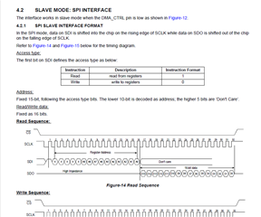
And i have to achieve the sequence attached in the image. 

Thank you  

Parents
  • Hi,

    I recommend you use the SPI master driver, which will handle everything for you. The SPI hardware peripheral and SPI driver count 8 bit words but that does not have any practical implication for what happens on the SPI line. How you think of the data is up to you, whether you think of it as a single 16 bit word or two 8 bit words has no implication on the physical data on the SPI bus.

  • I realized that first i should understand the SPI examples provided in the SDK thoroughly before customizing them.

    I am using nrf52832 DK as Master and flashing SPI example to it which is supposed to send a string " NORDIC " and then i am flashing SPIS example to my nrf52840 DK which should act as the slave then.  Now, though the transactions are getting completed in both the kits and LED's get toggled but i am not receiving the string "NORDIC" from my slave . What do i have to modify in the slave example to receive the string ?

    #include "sdk_config.h"
    #include "nrf_drv_spis.h"
    #include "nrf_gpio.h"
    #include "boards.h"
    #include "app_error.h"
    #include <string.h>
    
    #include "nrf_log.h"
    #include "nrf_log_ctrl.h"
    #include "nrf_log_default_backends.h"
    
    #define SPIS_INSTANCE 1 /**< SPIS instance index. */
    static const nrf_drv_spis_t spis = NRF_DRV_SPIS_INSTANCE(SPIS_INSTANCE);/**< SPIS instance. */
    
    #define TEST_STRING "Nordic"
    static uint8_t       m_tx_buf[] = TEST_STRING;           /**< TX buffer. */
    static uint8_t       m_rx_buf[sizeof(TEST_STRING) + 1];    /**< RX buffer. */
    static const uint8_t m_length = sizeof(m_tx_buf);        /**< Transfer length. */
    
    static volatile bool spis_xfer_done; /**< Flag used to indicate that SPIS instance completed the transfer. */
    
    /**
     * @brief SPIS user event handler.
     *
     * @param event
     */
    void spis_event_handler(nrf_drv_spis_event_t event)
    {
        if (event.evt_type == NRF_DRV_SPIS_XFER_DONE)
        {
            spis_xfer_done = true;
            NRF_LOG_INFO(" Transfer completed. Received: %s",(uint32_t)m_rx_buf);
            printf("recieved : %s", m_rx_buf );
        }
    }
    
    int main(void)
    {
        // Enable the constant latency sub power mode to minimize the time it takes
        // for the SPIS peripheral to become active after the CSN line is asserted
        // (when the CPU is in sleep mode).
        NRF_POWER->TASKS_CONSTLAT = 1;
    
        bsp_board_init(BSP_INIT_LEDS);
    
        APP_ERROR_CHECK(NRF_LOG_INIT(NULL));
        NRF_LOG_DEFAULT_BACKENDS_INIT();
    
        NRF_LOG_INFO("SPIS example");
    
        nrf_drv_spis_config_t spis_config = NRF_DRV_SPIS_DEFAULT_CONFIG;
        spis_config.csn_pin               = APP_SPIS_CS_PIN;
        spis_config.miso_pin              = APP_SPIS_MISO_PIN;
        spis_config.mosi_pin              = APP_SPIS_MOSI_PIN;
        spis_config.sck_pin               = APP_SPIS_SCK_PIN;
    
        APP_ERROR_CHECK(nrf_drv_spis_init(&spis, &spis_config, spis_event_handler));
    
        while (1)
        {
            memset(m_rx_buf, 0, m_length);
            spis_xfer_done = false;
    
            APP_ERROR_CHECK(nrf_drv_spis_buffers_set(&spis, m_tx_buf, m_length, m_rx_buf, m_length));
    
            while (!spis_xfer_done)
            {
                __WFE();
            }
    
            NRF_LOG_FLUSH();
    
            bsp_board_led_invert(BSP_BOARD_LED_0);
        }
    }
    

  • Hi,

    I do not see any problems with this code. I think we need two things in order to understand more:

    • Datasheet of the SPI slave (what is it?) so that we can check if you have set the correct SPI mode.
    • Logic analyzer trace of the SPI lines so that we can see what is actually going on.
  • Hi Einar,

    Thanks for helping me with this. PFA the datasheet and an image where you can read about the modes. I assume, it says the data will be shifted on SDI using SPI mode 2 and on SDO using SPI mode 3. isn't that right? So once I write the data on SDI line, would i have to uninitialize the SPI first to configure it to mode 3 or can i directly change the mode ? 

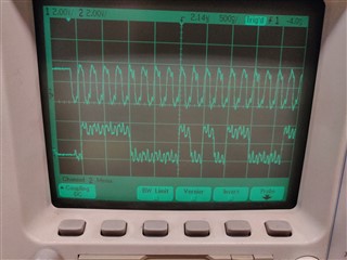
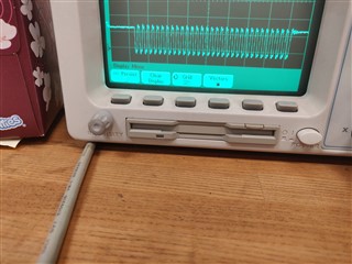
    Also, find attached the trace of SCK and MOSI SPI lines.

    Can you figure out whats going wrong?

    Appreciate it!!

    Atmel-46004-SE-M90E36A-Datasheet.pdf

  • Hi Einar,

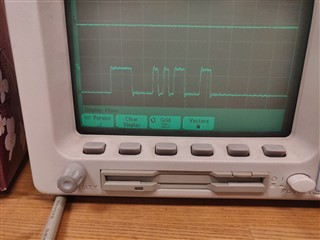
    One more trace of when I send 0X00305678 / 0b00000000001100000101011001111000

  • Hi,

    Yes, it seems like it uses both SPI mode 2 and 3. Essentially that means that you have to uninit and reinitialize the SPI driver with a new configuration every time you switch between read and write. I would expect that to work.

  • Hi Einar,

    How can I achieve this ? I want to have a 32 bit transaction but first 16bits should be on SPI mode 2 and other 16bits on SPI mode 3. How do I uninitialize and reinitialize in between the transaction ? 

Reply Children
  • Hi,

    To reinitialize you have to uninitialize the driver using nrf_drv_spi_uninit() then initialize it again with nrf_drv_spi_init() with the new configuration.

    Br,

    Einar

  • Hi Einar,

    Yes, I got that one but I am not sure where to start uninitializing and re-initialize the SPI with new configuration. If you see the attached read sequence. I have to write first 16bits in mode 2 and then receive 16bits in SPI mode 3. And it should not be 2 different 16 bits transaction , instead one 32 bits transaction. How can I achieve this ?

  • Hi,

    You cannot switch mode just like that. However, I would assume that the slave device would not matter that there is a delay between the first 16 and last 16 bits, as the clock is anyway generated by the master. The idea is that after transmitting the first 16 bits you initialize the driver to use another mode and receives the 16 bits. It would stretch the transaction so that it looks something like this:

  • Thanks Einar for the explanation, 

    Is this the correct implementation to achieve what you showed in the diagram above ? 

                                                         nrf_drv_spi_transfer (spi, first 16bit data, 2, first 16bit data, 2);

                                                         unint spi

                                                         spi mode-> 3

                                                        nrf_drv_spi_transfer (spi, last 16bit data, 2, last 16bit data, 2);

    I am just confused with the length parameter. if I am specifying 2 bytes of length, will that mean that the CS line will go high after writing 2 bytes ? if that is true, then this implementation will obviously not work. 

    Regards,

  • Hi,


    The "nrf_drv_spi_transfer" function will set the CSN active prior to the first byte written. If you require the CSN pin to be kept low (ie: active), then you need to manually control the GPIO. This is done by setting "spi_config.ss_pin = NRF_DRV_SPI_PIN_NOT_USED", then controlling it manually in your own transfer function.

    Best regards,

    Håkon

Related