This post is older than 2 years and might not be relevant anymore
More Info: Consider searching for newer posts

nrf52832 4 layers pcb antenna trace design

I design a 4 layer pcb which include nrf52832. But i'm unsure what rf trace width should be on 4 layers pcb? 

This trace 30mil width and 5mil clearance for 2 layers pcb as discussed here: https://devzone.nordicsemi.com/f/nordic-q-a/23011/nrf52832-antenna

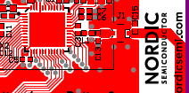
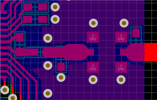
that's ok. I have also nrf52 DK. This is a 4 layers pcb. As i know layer2 ground but keepout under rf trace,also layer3 keepout. RF trace on layer1 referenced layer4 ground and calculated refer to layer4, am i right? 

Why rf trace width variable(start thin,go thicker),not constant? And how is it calculated to ensure 50ohm impedence? 

Berker ISIK

Best Regards

  • Technically, you don't need to have the cutout under on  the inner layers, the capacitance to ground is low with just the footprint of two components. If you use a transmission line between L1 and the antenna, you need to calculate it using the specification for the board you are using. It's sometimes easier to remove the inner layer because the distance to the inner layers doesn't matter and you don't lock your design to one specific stack up. 

    The wider track on the DK is the 50 ohm transmission line. It's on the short side so is debatable whether is has an impact or not. 

    The easiest is to use a co-planar waveguide. You can find on-line calculators or use Appcad to calculate the dimensions. The important parameters are distance to the same side ground plane, distance to the other or inner side ground plane and the track width.

  • Hi,

    Layer4 is not a continuous ground layer,there's some signals on it. As i know, ground layer under co-planar waveguide should be whole ground. 

    Why layer2 didn't used instead of layer4? This is a whole ground. 

    I think if layer2 is used, the calculations should change completely. 

    Note: I calculated thinner and thicker part impedances. These are about 58ohm and 48ohm respectively.

    Thickness of layer2 0.18mm. 

  • Yes,  you need to have a solid ground plane under the waveguide. If you can't use layer 4, use another layer and re-calculate the width.

  • Ji ,

    I don't want to take more your time. But I want to understand DK design. 

    Yes,  you need to have a solid ground plane under the waveguide

    Yes,  you need to have a solid ground plane under the waveguide

    Layer4 on DK,is not a solid plane. 

    Layer1:Sİgnal

    Layer2:GND

    Layer3:PWR+Signal

    Layer4:GND+Signal

    How is calculated the impedance, although layer4 is not a solid ground?

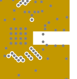
  • Yes, the bottom layer is solid under the RF section: 

    What happens on the rest of the board doesn't matter here.

Related