Good morning everyone,
I am struggling since a few days to understand how the SPI communication is supposed to work in the SDK 15.0.0....
So far, I am having some issues in understanding the documentation, so I hope you can help me figuring out what is wrong.
I have an external radio (semtech SX1261) attached to my NRF52832 Development Kit, and after having properly connected all the cables, I am trying to use the SPI to communicate
with the SX1261.
With the current configuration, I am trying to read the Packet type register and to configure it according to my needs. To check the functionality of the procedure I wrote a dummy code which periodically reads the current packet type setting and switches it every second. This snippet of code is attached below (the value like RADIO_GET_PACKETTYPE are correctly defined in an external file)
    uint8_t data = RADIO_GET_PACKETTYPE;
    uint8_t data2[2] = {RADIO_SET_PACKETTYPE, PACKET_TYPE_LORA};
    uint8_t data3[2] = {RADIO_SET_PACKETTYPE, PACKET_TYPE_GFSK};
    uint8_t m_rx_buf[2];    /**< RX buffer. */
    bool alternate = false;
    while (1)
    {


   //     SX126xTestLbe_Tx();

        // Reset rx buffer and transfer done flag
        memset(m_rx_buf, 0, 16);
        spi_xfer_done = false;
        if (alternate)
        {

            APP_ERROR_CHECK(nrf_drv_spi_transfer(&spi, &data, 1, m_rx_buf, 2));
            nrf_delay_ms(50);
            APP_ERROR_CHECK(nrf_drv_spi_transfer(&spi, data2, 2, NULL, 0));
            nrf_delay_ms(50);
            APP_ERROR_CHECK(nrf_drv_spi_transfer(&spi, &data, 1, m_rx_buf, 2));
            alternate = false;
        }
        else
        {

            APP_ERROR_CHECK(nrf_drv_spi_transfer(&spi, &data, 1, m_rx_buf, 2));
            nrf_delay_ms(50);
            APP_ERROR_CHECK(nrf_drv_spi_transfer(&spi, data3, 2, NULL, 0));
            nrf_delay_ms(50);
            APP_ERROR_CHECK(nrf_drv_spi_transfer(&spi, &data, 1, m_rx_buf, 2));
            alternate = true;
        }
    //    APP_ERROR_CHECK(nrf_drv_spi_transfer(&spi, m_tx_buf, m_length, NULL, m_length));

}
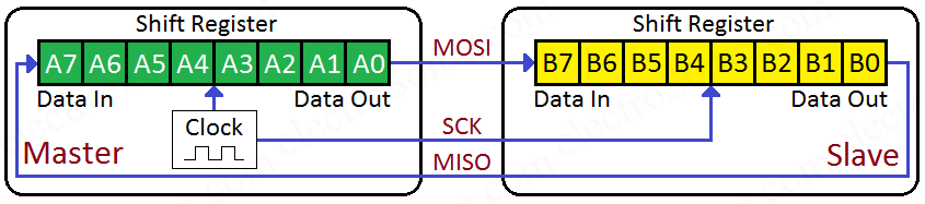
The syntax of the read command is supposed to be the following on the SPI: 1 clock for the MOSI to write the command "RADIO_GET_PACKETTYPE" and another clock for the slave to reply with the current packet type (0x00 or 0x01)
On the logic analyzer (screenshot below) you can see that the MOSI line is already responding when the MOSI is supposed to write, and no reply is coming as the second byte. Furthermore, the master seems to be sending an 0xFF on the second clock.

If in the command APP_ERROR_CHECK(nrf_drv_spi_transfer(&spi, &data, 1, m_rx_buf, 2));
I increase the rx_read parameter from 2 to 3 as follows APP_ERROR_CHECK(nrf_drv_spi_transfer(&spi, &data, 1, m_rx_buf, 3));
then I got the correct value read as the third byte, as shown in the logic screen capture below. I still don't understand why I have readings on the first 2 bytes from the MISO, though.....
Furthermore, I cannot understand why a 3rd byte is required....according to the infocenter, the command above should generate 4 clocks....right?

And finally, I am not entirely sure I understood the difference between SPIM, SPI, NRFX_SPI and so on, with relative confusion when reading the documentation....
I hope you can help me figuring out what I am doing wrong.
This is my sdk_config.h for the components in use for the SPI
// <e> SPI0_ENABLED - Enable SPI0 instance
//==========================================================
#ifndef SPI0_ENABLED
#define SPI0_ENABLED 1
#endif
// <q> SPI0_USE_EASY_DMA  - Use EasyDMA


#ifndef SPI0_USE_EASY_DMA
#define SPI0_USE_EASY_DMA 1
#endif

/**********************************************/


// <e> NRFX_SPIM_ENABLED - nrfx_spim - SPIM peripheral driver
//==========================================================
#ifndef NRFX_SPIM_ENABLED
#define NRFX_SPIM_ENABLED 1
#endif
Thank you for your help!