
Hi all,
I am new to the EE/hardware world. Coming from the CS side, I am trying to grasp little bit of knowledge every day.
I looked at the reference designs and am using the qfaa reference file. Since I am planning to build a board for BLE application:
- I should be referring to nrf51822_qfaa_pcb and not _1v8 or _dcdc. Right?
- I want to attach a coin cell battery (3V) and because VDD and AVDD are all the same net, VCC_nRF, can I route it like this: (two images below)
Image 1:
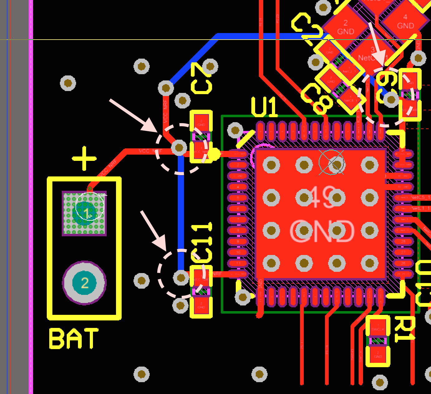
Image 2:
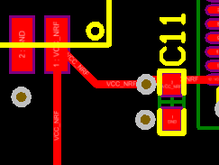
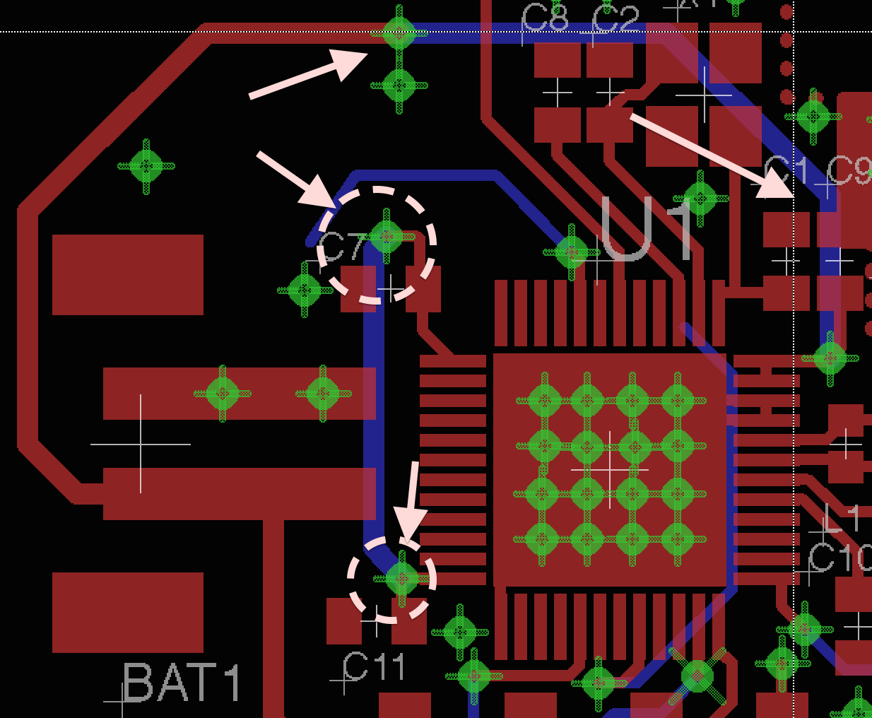
- What if I do this connect AVDD to battery and leave VDD connected to each other:
Image 3:
- Also when should I use VDD vs AVDD
I know these are beginner questions. Thanks for taking the time :)
Thanks! -IP

