Beware that this post is related to an SDK in maintenance mode
More Info: Consider nRF Connect SDK for new designs
This post is older than 2 years and might not be relevant anymore
More Info: Consider searching for newer posts

Reading WS2812b leftover data through I2S

Hello there,

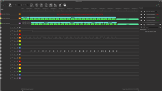
I am currently trying to read the leftover WS2812b LED strip data which was sent using a single channel I2S. The data sent from the board (through I2S) looks like this:

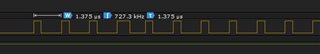
with around 34 mV for high and around 2~6 mV on low. I decided not to send FFF, but 888 instead.

I am aiming to calculate the length of the LED strip. Each LED chip will read the first 24 bits of the data, cascade (discard) it, then pass it to the next one. Therefore, the strategy is to get the data after being cascaded by the last chip and calculate the length of it (which later will be divided by 24 to see how many are left).

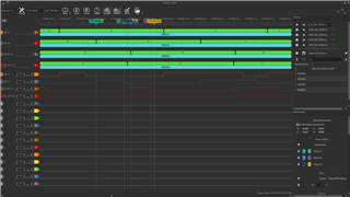
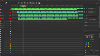
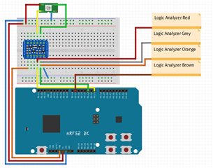
The question is: How will I be able to read those data? I tried reading as usual (set a buffer for the i2s, start it, listen for it (delay), stop it, then check its buffer), but I got my buffer filled with all FFF instead. and a thing is that... when I tried to read anything from the pin, although I am not sending any data (the LED strip is not powered on, but connected to other's ground), there will be data, which should not happen. I assigned pin 22, 23, 24, 25 to be the i2s input pin (which will be assigned and unassigned when used or unused), and they are configured as follows:

nrf_gpio_cfg_sense_input(DIN1_PIN, NRF_GPIO_PIN_PULLDOWN, NRF_GPIO_PIN_SENSE_HIGH);

Thank you in advance.

Parents
  • Hi Einar,

    Sorry, please disregard 34 mV and 2~6 mV, it's wrong, it should be 2.79 V for High and -15.9 mV (or 0 V) for Low. This is the data signal created on WS2812B's Data out.

    I connected the strip directly to the board's VDD to power it on, P0.11 for Data, and ground. I did not use any level converter (I know that I'm suggested to supply 5v and use a level converter, but 3.3 V is able to turn the LED on so, I'm trying it).

    When there is no data being transferred through the WS2812b, the voltage of the DOUT is around -0.8 mV ~ -78.92 mV. At this state, if I call the board to read any data, by using

    i2s_config_init(DIN2_PIN, 17);

    where DIN2_PIN is defined by

    #define DIN2_PIN 23

    , followed by

    i2s_start();
    nrf_delay_us(I2S_DETECTION);
    
    for (i = 1; i < I2S_BUFFER_SIZE; i++) {
    	if (I2SRxBuffer[i] != 0 || I2SRxBuffer[i] != -1) {
    		printf("isi: %x\r\n", I2SRxBuffer[i]);
    		printf("as: %d\r\n", I2SRxBuffer[i]);
    		if (I2SRxBuffer[i] > 0x11111110) {
    			lengthz++;
    		}
    	}
    }
    
    i2s_stop();

    , I2SRxBuffer[i] will always print ffffffff.

  • Hi,

    OK. The logical levels for the nRF are supposed to be above 0.7 * Vdd for high and below 0.3 * Vdd (but > 0 V) for low. However, I would not expect that the logical levels are OK for the nRF, and the low negative voltage for logical '0' should be ok. But I would not do it like this in an actual end product.

    I do not have any idea if the voltages are acceptable to the WS2812b, though. It is out of spec after all (according to the datasheet it should be between +3.5 and +5.3). Can you show us logic analyzer plots of the data out of the WS2812b? Is it all FF's there as well? If so then I would try using a level shifter and supplying the WS2812b with a voltage within spec before digging any further.

    By the way, are you basing your endeavors on this blog post?

  • Alright, I found one which is able to do 100 MHz. Otherwise, I do not want to believe this.

    Here's the capture:

    The order is the same with the previous logic analyzer capture.

  • Perfect. But now I am having trouble understand in what I am looking at. Can you explain in detail which signal in this plot is supposed to follow which, how they are connected etc.? It is difficult to see the timing etc. from the plot.

    Generally, PPI behaves as I explained, and that is deterministic. Of course, there can be some jitter depending on the input signal relative to the internal 16 MHz peripheral clock, but that is all. Any other noise must be caused by something else.

  • Okay, Here's the improved capture. The 4 lines above are the decoded version of the 4 lines below. The color on the left represents their connection (brown with brown, purple with purple).

    Please note on the lower right part, below Cursor Distance. Those are the time sampled.

    1-2 belongs to the original data, LED Out

    3-4 belongs to the Self PPI out

    5-6 belongs to the Other PPI Out

  • Generally, PPI behaves as I explained, and that is deterministic. Of course, there can be some jitter depending on the input signal relative to the internal 16 MHz peripheral clock, but that is all. Any other noise must be caused by something else.

    I agree with this. Otherwise, I believe PPI should not behave like what I experience, right?

Reply Children
Related