This post is older than 2 years and might not be relevant anymore
More Info: Consider searching for newer posts

How to implement two TWI instances

Hello,

I am having difficulty using a single TWI to support a DAC (MCP4725) and IMU (BNO055). 

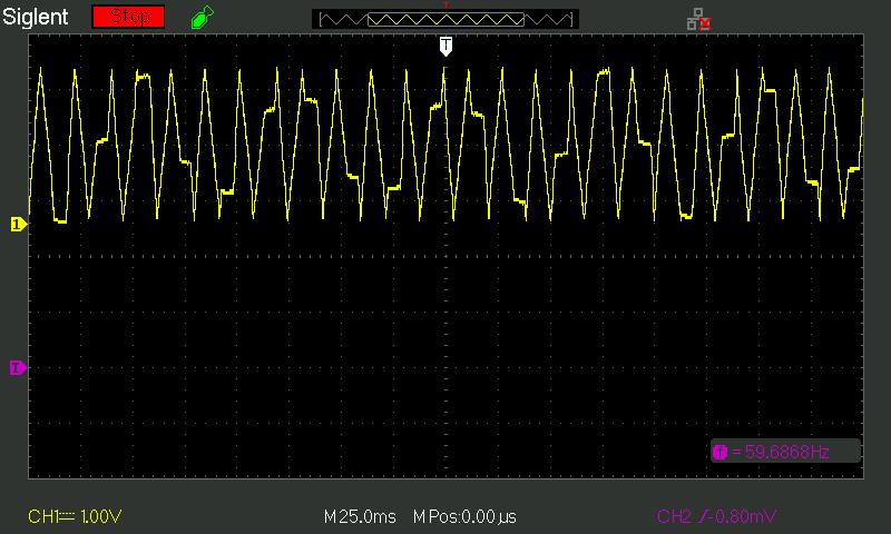
I am using nRF52 DK, and SDK 14.3 with the SEGGER IDE.  The DAC is running on a timer with samples being loaded every 200 micro seconds.  The IMU is running on the same TWI bus and I am collecting 3 data samples (2 bytes each) every 20 milliseconds.  The data is being piped over BLE at 50 samples per second (packing 2 sets of samples in a single 20 byte packet every 40 milliseconds). If I output a triangular waveform, I get an artifact every 20 milliseconds with a varying time for the length of the artifact (see the attached images below).  

My plan is to split the processing so the DAC is on one twi and the IMU on a second TWI bus.  If I do this, what pins can be used for the second TWI if I use the default pins for the first TWI?  Below are my initialization functions:

void dac_twi_init (void)
{
ret_code_t err_code;

const nrf_drv_twi_config_t twi_mcp4725_config = {
.scl = ARDUINO_SCL_PIN,
.sda = ARDUINO_SDA_PIN,
.frequency = NRF_TWI_FREQ_400K,
.interrupt_priority = APP_IRQ_PRIORITY_HIGH,
.clear_bus_init = false
};

err_code = nrf_drv_twi_init(&m_dac, &twi_mcp4725_config, twi_handler, NULL);
APP_ERROR_CHECK(err_code);


nrf_drv_twi_enable(&m_dac);
}

void imu_twi_init (void)
{
ret_code_t err_code;
const nrf_drv_twi_config_t twi_bno055_config = {
.scl = 10,
.sda = 9,
.frequency = NRF_TWI_FREQ_400K,
.interrupt_priority = APP_IRQ_PRIORITY_HIGH,
.clear_bus_init = false
};

err_code = nrf_drv_twi_init(&m_imu, &twi_bno055_config, twi_bno055_handler, NULL);
APP_ERROR_CHECK(err_code);

nrf_drv_twi_enable(&m_imu);
}

As you can see, the amount of corruption in the waveform varies.  Sometimes it is very obvious and sometimes almost undetectable.  Occurring every 20 mS indicates that the transfer of data from the IMU is impacting the ability for the DAC outputs to continue at the 200 microsecond intervals (they get delayed and thus the horizontal corruption in the DAC output).

My questions are:

1. Do you think using 2 TWIs will solve the issue?

2. Are Pins 9 and 10 "legal" pins to use for the second TWI?

3. Does my initialization above look correct?

4. Is there a possibility of other causes of the corruption and what are they?

Thanks in advance for your help.  This medical project is in the final prototype stages and "clean" DAC waveforms are absolutely necessary.
 

  • Hi Gary

    Have you tried to scope the TWI lines to see how the TWI transactions are scheduled?

    Are you sure that there is enough time to read both the sensors within the same interval?

    Is the DAC being read every 200us, or does it buffer multiple samples before you have to read them out?

    1. If the problem is bus bandwidth then using 2 TWI's should solve the problem, but it is possible you could also solve it by finding a different way to schedule the TWI access (by making sure you wait for the next DAC transaction before servicing the IMU for instance). 

    2. Yes, any GPIO on the nRF52832 can be used for TWI. 

    3. Assuming you initialize the m_imu variable using a unique index in the NRF_DRV_TWI_INSTANCE(x) macro, then it should be correct. 

    4. Without knowing more about your system I don't want to speculate too much. Is the timer sampling the ADC internal in the ADC, or controlled from the Nordic device?

    Best regards
    Torbjørn

  • Thank you for your prompt response Torbjorn,

    I will scope out the TWI lines and let you know my findings.  

    There is an option in the nrf_twi.h file for 800kbps operation that has been commented out - can that be used?  

    typedef enum
    {
    NRF_TWI_FREQ_100K = TWI_FREQUENCY_FREQUENCY_K100, ///< 100 kbps.
    NRF_TWI_FREQ_250K = TWI_FREQUENCY_FREQUENCY_K250, ///< 250 kbps.
    NRF_TWI_FREQ_400K = TWI_FREQUENCY_FREQUENCY_K400, ///< 400 kbps.
    //NRF_TWI_FREQ_800K = TWI_FREQUENCY_FREQUENCY_K800 ///< 800 kbps
    } nrf_twi_frequency_t;

    Also, I used 10k pullups for the SDA/SCL lines and I found your spec calls out for less than 7k - I plan to change it to around 5k. Do I need to beef up the GPIO output to handle a 5k pullup resistors?

    There are no reads from the DAC, only writes based on an app timer going off every 200 micro seconds.  The IMU is read for six 16 bit samples running on a separate app timer at 20 milliseconds.  The IMU only requires 128 clock cycles to transfer the data in from the IMU but one point I will check is to see if the IMU promptly responds to the read request - if not, then the TWI bus may be locked up waiting on the IMU.  Do you agree that using a second TWI master can resolve the issue and not impact the other TWI?

    I do have four ADCs running on internal clocks for other data collection but that only happens every couple of seconds.  Can the "independent" running of ADC collection impact the timing on the TWI channels? 

    I also have PWM being generated at varying duty cycles (1 to 10 %) at frequencies up to 20 K Hz.  Again, the frequency of corruption does not correlate to the PWM generation.

    I will check on the using a unique index in the NRF_DRV_TWI_INSTANCE(x) macro - I am not sure how to do that but will let you know if I need additional help to check that.

  • Thanks for the hint on posting code - will try that next time.

Related