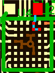
Routing the DCC pin on the nRF52832 with the chip scale package is pretty tough. The bump is surrounded on all sides by other bumps, so I don't have room for a via in the PCB process I'm using. I am wondering if I can route this trace along the path that connects with GPIO pins for P0.31 (B5) and P0.40 (A5)? Will that mess up the chip operation or will it be ok if I don't plan on using those GPIOs?