This post is older than 2 years and might not be relevant anymore
More Info: Consider searching for newer posts

SPI AND SPIM READING ISSUES

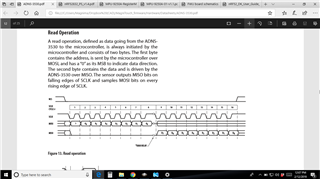
hi all i am trying to read data from a sensor in burst mode i can"t able to read all datas from the register .I tried to read the data in both spi and spim(with easydma) . spim is more better it reads data from 2 register(i am trying to read data of 3 register using burst mode).how can i solve this issues.

Parents
  • I assume you control NCS correctly, setting low before the first of two transfers and only high after the second with the 4 uSec delay between the two transfers. However your code shows that you are also telling the nRF SPI code to take control of NCS. Here is the default setting for NCS and the handler for init:

    // Starts by assuming NCS is not required
    
    /**
     * @brief SPI master instance default configuration.
     */
    #define NRF_DRV_SPI_DEFAULT_CONFIG                           \
    {                                                            \
        .sck_pin      = NRF_DRV_SPI_PIN_NOT_USED,                \
        .mosi_pin     = NRF_DRV_SPI_PIN_NOT_USED,                \
        .miso_pin     = NRF_DRV_SPI_PIN_NOT_USED,                \
        .ss_pin       = NRF_DRV_SPI_PIN_NOT_USED,                \
        .irq_priority = SPI_DEFAULT_CONFIG_IRQ_PRIORITY,         \
        .orc          = 0xFF,                                    \
        .frequency    = NRF_DRV_SPI_FREQ_4M,                     \
        .mode         = NRF_DRV_SPI_MODE_0,                      \
        .bit_order    = NRF_DRV_SPI_BIT_ORDER_MSB_FIRST,         \
    }
    
    // Tests if NCS is not required
    
        // - Slave Select (optional) - output with initial value 1 (inactive).
        if (p_config->ss_pin != NRF_DRV_SPI_PIN_NOT_USED)
        {
            nrf_gpio_pin_set(p_config->ss_pin);
            nrf_gpio_cfg_output(p_config->ss_pin);
        }
        m_cb[p_instance->drv_inst_idx].ss_pin = p_config->ss_pin;


    However your code shows that you are requesting the nRF SPI driver to take over NCS:

    spi_config.ss_pin = SPI_MOUSE_CSN_PIN;

    The nRF handler will now drive NCS low before and high after every transaction, including between the two transactions you require, for example sww nrf_drv_spi.c

    static void finish_transfer(spi_control_block_t * p_cb)
    {
        // If Slave Select signal is used, this is the time to deactivate it.
        if (p_cb->ss_pin != NRF_DRV_SPI_PIN_NOT_USED)
        {
            nrf_gpio_pin_set(p_cb->ss_pin);
        }


  • so i want to remove this  "spi_config.ss_pin = SPI_MOUSE_CSN_PIN;" portion from the code  then only i get correct data from burst mode read.

  • sir i changed tx_bm_dummy to NULL in second call to nrf_drv_spi_transfer, and set the tx_length parameter to 0 put datas are not getting i don't known why

  • sir is there any major difference between spi and spim data transfer except that easydma involvement 

  • SIR WHEN I USED SPI (NOT SPIM "SPI0_USE_EASY_DMA 0 "IN  sdk_config.h) AND NORMAL READ OPERATION THE VALUES FROM ALL THREE REGISTER GETTING PROPERLY.I WILL PLACE THE CODE FOR NORMAL READ BELOW

    ////////////////////////////////////////////////////////////////////////////////////////////////////////////////////////////////////////////////////////////////////

    uint32_t adns_reg_read(const nrf_drv_spi_t * i_spi_address,uint8_t i_reg, uint8_t *io_data)
    {
    uint32_t err_code;

    /* Read operation. See ADNS-3530 datasheet (p.12).

    A read operation, defined as data going from the ADNS-3530 Sensor to the
    micro-controller, is always initiated by the micro-controller and consists
    of two bytes. The first byte contains the address, is sent by the micro-controller
    over MOSI, and has a "0" as its MSB to indicate data direction. The second byte
    contains the data and is driven by the ADNS-3530 Sensor over MISO. The sensor outputs
    MISO bits on falling edges of SCLK and samples MOSI bits on every rising edge of SCLK.

    */
    uint8_t tx_data[2];
    uint8_t rx_data[2];

    // Reset serial port
    adns_ncs_assert(i_spi_address,1); //disable ncs
    adns_ncs_assert(i_spi_address,0); //enable ncs

    if(i_spi_address == NULL | io_data == NULL)
    {
    return NRF_ERROR_INVALID_PARAM;
    }

    // The MSB to "0" to indicate a read operation
    tx_data[0]= i_reg & 0x7f;
    tx_data[1]= 0xff; // Buffer to provide clock for rx data.

    // Send the address to read
    APP_ERROR_CHECK(nrf_drv_spi_transfer(i_spi_address,(const uint8_t *)&tx_data[0],1,&rx_data[0],1));

    nrf_delay_us(4); // tSRAD delay

    // Read the data by sending a dummy byte
    APP_ERROR_CHECK(nrf_drv_spi_transfer(i_spi_address,(const uint8_t *)&tx_data[1],1,&rx_data[1],1));

    adns_ncs_assert(i_spi_address,1); //disable ncs

    // Return the second byte from rx_data
    *io_data = rx_data[1];


    return NRF_SUCCESS;
    }

    /////////////////////////////////////////////////////////////////////////////////////////////////////////////////////////////////////////////////////////////////

Reply
  • SIR WHEN I USED SPI (NOT SPIM "SPI0_USE_EASY_DMA 0 "IN  sdk_config.h) AND NORMAL READ OPERATION THE VALUES FROM ALL THREE REGISTER GETTING PROPERLY.I WILL PLACE THE CODE FOR NORMAL READ BELOW

    ////////////////////////////////////////////////////////////////////////////////////////////////////////////////////////////////////////////////////////////////////

    uint32_t adns_reg_read(const nrf_drv_spi_t * i_spi_address,uint8_t i_reg, uint8_t *io_data)
    {
    uint32_t err_code;

    /* Read operation. See ADNS-3530 datasheet (p.12).

    A read operation, defined as data going from the ADNS-3530 Sensor to the
    micro-controller, is always initiated by the micro-controller and consists
    of two bytes. The first byte contains the address, is sent by the micro-controller
    over MOSI, and has a "0" as its MSB to indicate data direction. The second byte
    contains the data and is driven by the ADNS-3530 Sensor over MISO. The sensor outputs
    MISO bits on falling edges of SCLK and samples MOSI bits on every rising edge of SCLK.

    */
    uint8_t tx_data[2];
    uint8_t rx_data[2];

    // Reset serial port
    adns_ncs_assert(i_spi_address,1); //disable ncs
    adns_ncs_assert(i_spi_address,0); //enable ncs

    if(i_spi_address == NULL | io_data == NULL)
    {
    return NRF_ERROR_INVALID_PARAM;
    }

    // The MSB to "0" to indicate a read operation
    tx_data[0]= i_reg & 0x7f;
    tx_data[1]= 0xff; // Buffer to provide clock for rx data.

    // Send the address to read
    APP_ERROR_CHECK(nrf_drv_spi_transfer(i_spi_address,(const uint8_t *)&tx_data[0],1,&rx_data[0],1));

    nrf_delay_us(4); // tSRAD delay

    // Read the data by sending a dummy byte
    APP_ERROR_CHECK(nrf_drv_spi_transfer(i_spi_address,(const uint8_t *)&tx_data[1],1,&rx_data[1],1));

    adns_ncs_assert(i_spi_address,1); //disable ncs

    // Return the second byte from rx_data
    *io_data = rx_data[1];


    return NRF_SUCCESS;
    }

    /////////////////////////////////////////////////////////////////////////////////////////////////////////////////////////////////////////////////////////////////

Children
Related