This post is older than 2 years and might not be relevant anymore
More Info: Consider searching for newer posts

nRF52832 chip antenna validation

I have a problem with understanding reference layout for the chip antenna I want to use in my project. The antenna is ANT016008LCS2442MA2 from TDK.

Based on the schematic attached below:

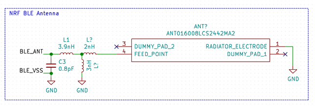
I have three questions:

1. Is RADIATOR_ELECTRODE correctly connected to GND?

2. Should I leave dummy pads not connected?

3. Is matching circuit correct? 

Parents
  • Hi,

    The radiator electrode is not connected to ground so you can let this pin unconnected in the schematics. If you take a look at the layout in the antenna datasheet the radiator electrode is connected only connected to a trace, but the trace is not connected to ground. I also found these designer notes, you should follow the dimensions for the keepout area around the antenna as specified here. The dummy pads should also be left unconnected.

    There are no changes needed for the matching circuits in your schematic, you have included both the RF matching components of the nRF52832 and a L matching network for the antenna as specified in the antenna datasheet. There are some recomendations for the values of the tuning components of the antenna in the design notes i linked above, but it will be difficult find the optimal values for these components before you perform a antenna tuning with a network analyzer.


    Best Regards,

    Marjeris

  • OK thanks for you answer. I was confused by the via's in the trace you mentioned. I assumed it's a coplanar waveguide with ground plane on the bottom layer. 

Reply Children
Related