
Hi,
I'm designing custom PCB with nRF52832QFAA chip and after custom PCB population I can't make SWD to get working. In order to eliminate where the issue is I would like to start to populate as few components on PCB as possible in order to make chip alive, then add the rest. My question is, will the bare chip start working (SWD) with just 32MHz crystal and loading caps?
Thank you.
Peter


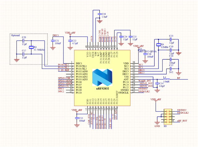 emaining - do you mean caps on DEC1, DEC3, DEC4 ?
