This post is older than 2 years and might not be relevant anymore
More Info: Consider searching for newer posts

nrf52840 pi hat

hi all

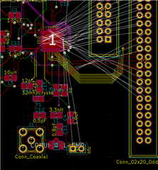
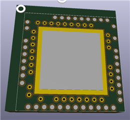
i have been working on a raspberry pi hat design and i would like feedback on it's design

this is the link to the github repo and i do update it regularly  https://github.com/sentinelinfinitus/nrf52840-pi-sheild

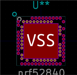
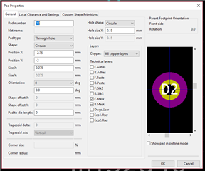
fair warning i used kicad and for some parts were added using mousers library loader

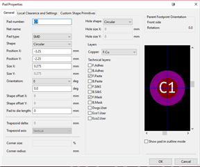
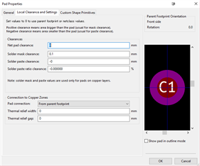
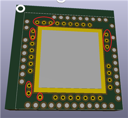
if you see some things i am doing wrong or have any suggestions on how to do some things better please let me know

Parents
  • Hi,


    DEC4 must be connected to DEC6, this was changed after v0.5 of the OPS was released, you might want to reference documentation which is up to date. https://www.nordicsemi.com/DocLib/Content/Product_Spec/nRF52840/latest/keyfeatures_html5


    For some reason I am not able to view the design layout, probably due to my own KiCad incompetence. Are you able to export gerbers or something else?


    Best regards,

    Andreas

  • chances are you don't have the parts added and thats why you can't see them

    all the parts in use are in the parts folder most of them you have to add via mousers part loader it will create a library that you will have to add manually

    there is one part that is not added via part loader for that one you just manually add it

    to add parts to the schematic view open the schematic view

    preferences>manage symbol library>browse library

    ex: nrf52840-qiaa       {pihatfolder}/kicad-library-master/kicad-library-master/schema-components/nrf52840-qiaa.lib

    ex:[SamacSys_Parts aka mouser parts lib] C:/libloader/SamacSys_Parts.lib this is where mine is

    to add the footprints open footprint library editor

    preferences>manage symbol library>browse library

    ex:[SamacSys_Parts again the mouser parts] C:/libloader/SamacSys_Parts.mod

    ex: RuuviTag    /nrf52840 pi sheild/kicad-library-master/kicad-library-master/RuuviTag.pretty [please note this one is a folder]

    also there is a hat.pdf it's the schematic in pdf format this is what i assume you are referencing in the quoted section
    {quote}

    [For some reason I am not able to view the design layout, probably due to my own KiCad incompetence. Are you able to export gerbers or something else?[

  • Hi,


    I updated my KiCad application, that seemed to do the trick. Please verify that what I am seeing is correct though:


    This is not good, and probably will not work at all. I recommend that you take a look at our reference layout, there are pdf files which you can look at. Rotate the nRF 90 degrees clockwise so that the ANT pin points towards the RF components and place components similar to the reference layout. You have loads of available space, there is no reason to place components all over the place.

    When the ref. layout is replicated you can route GPIOs to targets on their respective side. If any pins are to be connected to anything on the opposite side of the chip it is better to see if you can re-assign the trace to a GPIO on the side which points towards the target, instead of routing a bunch of traces around the chip.

    Lastly, add a ground pour in the outer layers and connect all component ground pads directly to it, no wire grounding.


    Best regards,

    Andreas

  • I plan on redoing part of it anyway but at the moment I can't my pc has been disconnected for the moment and I have ordered a few upgrade parts that have shipped today

  • Hi,


    OK no problem, I can look over it once you have redone it. As mentioned though you should replicate the reference layout as closely as possible. There is no need to reinvent the wheel, you will just risk inventing new bugs or ways to degrade the RF power.


    You can find the reference layout here: https://www.nordicsemi.com/Products/Low-power-short-range-wireless/nRF52840


    Best regards,

    Andreas

Reply Children
  • well i started to impliment the new documentaion and i have learned the part i am using does not have all the pins on it so it looks like i will have to learn how to make custom parts for kicad

  • Hi,


    Unfortunately we do not have any experience with KiCad. I did a quick web search though, seems you should be able to find some nRF52840 libraries which you might be able to use (if this is not what you have done already).


    Best regards,

    Andreas

  • hi Andreas

    unfortunately i was using library's that i found online but they were missing pads on the footprint/schematic

    that being said i have taken the time to learn how to make parts and have created the part to the best of my ability (it came out as good as i thought it would)

    if you want to take a look at the part in the editor the same library adding instructions i had before should work as long as you use the location of the part i created

    the part is in the parts folder under the folder [sentinel]

    here is what i have though

    here is what the footprint looks like

    this is the settings for the red pads

    red pad settings

    this is the clearances of the red pads

    the yellow pad settings (please note they are through hole because that was the only way i could get them go to other layers)

    yellow pad clearance

    3d

    i know it does not follow the aqf73 guideline too well but it was the best i could do based on my limited experience with making kicad parts

    it would be nice if in the future nordic made kicad parts available in the future or if nordic want to make this part available to people i would not mind

  • Hi,


    This looks quite good. As you say, the reference design uses blind/micro vias in the inner-row pins. This is to make sure the SoC has good ground in that the center pad is connected to a solid plane in either inner or bottom layers. By using through hole vias this will no longer be the case, the vias wil break up the ground plane which might keep certain sensitive parts in the SoC from operating as specified.

    There are some ways to workaround this, by not using all the inner-row pins there will be better grounding overall. In addition there are some pins that you easily can route outside through the top layer. The ANT pin and the VSS_PA pin should also not have vias in them.

    I have also seen examples of designs where the inner-row pins have been routed out in the top layer between the pads of the outer-row pins. This obviously will depend on the capabilities of your PCB supplier and EMS. You might also have to make the pads of the outer-row pins a little smaller.


    Best regards,

    Andras

  • hi Andreas

    i did fix the part so that there were no vias under any pads


    also i have created the basic hat and even exported it's gerber files there in the hat\basic hat folder

    would you mind taking a look at it to see if the pcb is good


    something to make note of is hat you can do micro vias under pads in kicad by setting up a micro via off to the side and dragging it under the pad you want it under if you get a question about it in the future

Related