Hi,
As background, what I am trying to implement is continuous uninterrupted SPI master output from the nRF52840, compatible with the MCP4822 two-channel 12-bit DAC.
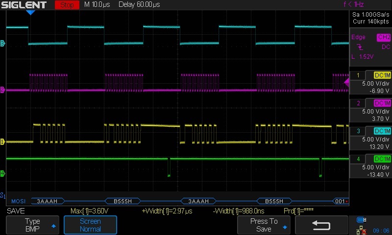
The MCP4822 requires programming waveforms from the nRF52840 as shown in this photo.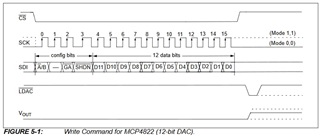
i.e. it requires two bytes of data to be sent via SPI while the CSN signal is low (to program one channel), followed by another two bytes of data to be sent via SPI while the CS signal is low (to program one channel), and then finally, it needs the LDAC signal to go low to cause the two analog outputs to change simultaneously.
The desired output frequency for this entire sequence is 16KHz, and I want too involve the CPU as little as possible in the process (as it will be busy doing other things.)
My understanding so far is that that the SPIM3 device is capable of controlling the CSN line, and that it can be used with EasyDMA in ArrayList mode.
I gather that the EasyDMA is limited to outputting a MAXCNT of 256 bytes, but that the ArrayList mode allows a list of pointers to contiguously allocated blocks of 256 bytes to be given to the EasyDMA, which allows it to transmit a longer burst of data.
It is not clear to me from the documentation how the timings of that data transmission are controlled.
For example:
What controls the SCK clock rate of the SPIM?
What controls how many bits/bytes of data are written out of the SPIM before the CSN line is brought high again?
What controls the time interval between successive SPIM writes (of 2-bytes each) from the ArrayList?
In order to allow contiguous transmission from the SPIM, I will need to have two memory "swing" buffers, wherein the CPU fills one buffer while the contents of the other is being transmitted by the SPIM. Then, when the transmission is complete, the buffers swap over and the process continues seamlessly.
I have several questions related to how to implement this.
Firstly I don't know how to trigger an interrupt routine when the SPIM's steadily incrementing TXD.PTR has exceeded a particular value within the ArrayList. (which will be longer than 256 bytes long)
Secondly, as there will typically be a delay between the interrupt triggering and the interrupt service routine (ISR) actually being executed, we need to allow the SPIM module to continue transmitting extra data from the buffer after the interrupt triggers, then, within the ISR read the TXD.PTR to see where the SPIM has actually go to, and use that value as the starting offset when the swing buffers are swapped over. The trouble is, I have no idea how to configure the SPIM and EasyDMA ArrayLists to behave this way, as I am lacking any detailed usage documentation.
For Example:
We could create two "swing buffer" EasyDMA ArrayLists, each with the capacity to transmit data for 30ms each. This could contiguously transmit a series of 20ms audio "frames".
If we fill the first 30ms capacity transmit buffer with 20ms of audio from frame 0, and 10ms from frame 1. The Easy DMA transmission is then started from the first buffer, address 0.
We then start filling a second 30ms buffer with 20ms of audio from frame 1 and 10ms from frame 2.
The interrupt is triggered when the TXD.PTR has reached the 20ms mark, but the SPIM continues to transmit subsequent data from the buffer until told otherwise.
The actual interrupt service routine is later entered and serviced at (say) 24ms. The EasyDMA transmission is then switched to start transmitting from the second buffer, at address 4ms.
The transfer between playing audio from the first buffer and playing audio from the second buffer is then seamless.
None of the above complexity would be required if the SPIM and EasyDMA supported ring-buffers, but oh well.
Finally, we have the issue of generating the LDAC pulses, which (ideally) need to be one SCK clock long, and synchronised with the end of each pair of SPIM transmissions.
I'm not sure how to implement this. Would something to do with the GPIOTE and PPI systems do the trick, perhaps if the timers were regularly re-synchronised within the ISR?
There are a number of errata involving the SPIM3 module, so answers that take those "gotchas" into account would be appreciated.
Regards,
Nicholas Lee