Hi,
I am trying to design the transmission lines based on the reference board design from Nordic.
I opened up the Altium layout file for the board which I downloaded from the website. I measured the RF trace width to be around 30 mils, and gap between ground and trace is around 11.6 mils. I looked at the layer stack-up, and found the board is FR4 with about 55 mils thick. I suppose this to be a grounded CPW waveguide, as it has copper at top and bottom layer with substrate in between. However, when I put numbers in the online calculator, the impedance value is around 70 Ohms.
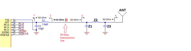
Second method to verify the impedance is that, I use the reference matching network and 50 Ohm ANT load, and calculate back to the source impedance. I also find the impedance is around 70 Ohms.
My question is, is the chip nRF52840 designed to be 50 Ohms load match? Should we design 50 Ohms TL to get the maximum output power efficiency? Why the transmission line I measured is about 70 Ohms rather than 50 Ohms?
Thanks for your help!