This post is older than 2 years and might not be relevant anymore
More Info: Consider searching for newer posts

Custom PCB - Nordic board layout spec question

Hi, guys. I copied the EAGLE schematic and PCB drawing file from the SparkFun nRF52832 Breakout design for my custom PCB (4 layers, FR-4).

https://cdn.sparkfun.com/assets/learn_tutorials/5/4/9/sparkfun-nrf52832-breakout-schematic-v10.pdf

https://www.sparkfun.com/products/13990

However, I wanted to refer to Nordic's PCBs. Also, I'm not used to reading the PCB Gerber files.
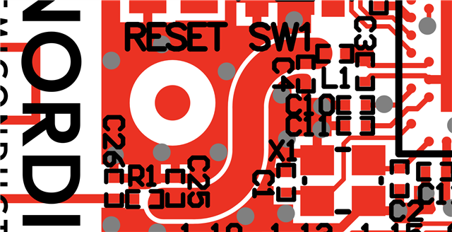
Q0. For the PCA10059 case (the nRF52840-QIAA dongle), I think this is a 2 layered board. The top copper is GND, isn't it?

Q1. For the PCA10059 case, what is connected to the bottom copper; 5V, 3.3V, GND?

Q2. For the PCA10059 case, what are the length and width of the impedance trace (L1 - C25)?

I'm surprised that the impedance trace is "curvy" because I thought this trace had to be a straight line.

Q3. For the PCA10059 case, what are the length and width of the PCB antenna trace?

Q4. What is the PCB thickness (height) of the PCA10059?

///////// Similarly
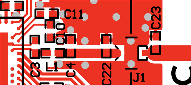
Q5. For the PCA10056 case (the nRF52840-DK 4 layered), what are each copper connected to?

Q6. For the PCA10056 case, what are the length and width of the impedance trace (C4 - C22)?

Q7. For the PCA10056 case, what are the length and width of the PCB antenna trace?

I noticed that both boards have different lengths and widths.

Also, I couldn't get a free Gerber file viewer for measuring these.

Q8. What is the PCB thickness (height) of the PCA10056?

Parents
  • Hi,

    Q0. For the PCA10059 case (the nRF52840-QIAA dongle), I think this is a 2 layered board. The top copper is GND, isn't it?

    Q1. For the PCA10059 case, what is connected to the bottom copper; 5V, 3.3V, GND?

     It varies, most of the bottom layer (blue) is GND while the top layer consist of different signals such as VDD, RF signal etc. I've included two images which shows the bottom and top layer.  


    Q2. For the PCA10059 case, what are the length and width of the impedance trace (L1 - C25)?

    I'm surprised that the impedance trace is "curvy" because I thought this trace had to be a straight line

    It's difficult to give you an exact measurement of the length since the transmission line is not straight, but a quick measurement gives approximate 300 mil (L1-C25). The width of the transmission line is approximately 35 mil. The reason for the curvy line is because it's designed to have a small form factor. We recommend to use a straight transmission line if you're not limited by mechanical requirements. 

    Q3. For the PCA10059 case, what are the length and width of the PCB antenna trace?

    Q4. What is the PCB thickness (height) of the PCA10059?

    A non precise measurement of the antenna length is 1100 mil, and antenna width 10 mil. The thickness of the board is around 81.5 mil.

    Q5. For the PCA10056 case (the nRF52840-DK 4 layered), what are each copper connected to?

    As in the previous design this varies. The bottom layer is a GND layer. The first mid layer (light blue) is mostly ground with some parts of it used to route signals from another layer. The second mid layer is GND layer. The top layer (red) is a signal layer, with ground on the centerpad. 

    Q6. For the PCA10056 case, what are the length and width of the impedance trace (C4 - C22)?

    The length of the transmission line (C4-C22)  is approximately 112 mil and the width of it is 30 mil. 

    Q7. For the PCA10056 case, what are the length and width of the PCB antenna trace?

    Approximately 990 mils length and 46 mil width. 

    I noticed that both boards have different lengths and widths.

    Also, I couldn't get a free Gerber file viewer for measuring these.

    The thickness of the DK is 62.992 mil. 

    Q8. What is the PCB thickness (height) of the PCA10056?

    The thickness of the DK is 62.992 mil. Although they both use the same IC (nRF52840) the PCA10056 and the PCA10059 is different in both thickness and width/length because they are made for two very different applications. The PCA10056 is a development board used to prototype an application and therefore is therefore designed on a bigger PCB. The PCA10059 is a USB dongle with a small form factor because it's limited by mechanical requirements. 

    I would like to repeat that the measurements are all approximations and are not precise, I therefore wouldn't recommend basing any design on these measurements. Antenna and matching network should not be copied from another design, the antenna used should be based on the requirements of the specific application: mechanical, range etc. The matching network should be matched to the specific PCB.

    Best regards

    Jared 

  • Thanks for your help!

    Antenna and matching network should not be copied from another design, the antenna used should be based on the requirements of the specific application: mechanical, range etc. The matching network should be matched to the specific PCB.

    Are you mentioning tools like AppCad?

    I am curious about what type of tools you guys use to get the drawing specifications.

  • Hi,

    Yes, AppCad is tool that is used by some of our engineers.

    Regards

    Jared 

  • Yes, AppCad is tool that is used by some of our engineers.

    Are there other tools you can recommend as well?

  • Altium, as most of our HW files are only available as Altium files

  • Hmm, do you mean that Altium provides tools when drawing 50 Ohm trace or 2.4GHz PCB antennas?

    Just like AppCad, I wish to ask whether there are extra programs/tools available for drawing 50 Ohm trace and 2.4GHz PCB antennas.

Reply Children
Related