This post is older than 2 years and might not be relevant anymore
More Info: Consider searching for newer posts

Optimizing PCB space with footprint size

Hi,

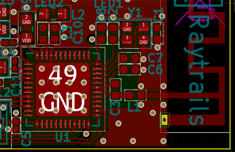
looking to nRF52832 reference PCB designs I've noticed that BOM contains different element sizes for different packages. Such, most of capacitors for QFN48 have 0402 footprint, when WLCSP suggests 0201. The same for crystals. So I'm thinking about saving some space with smaller packages.

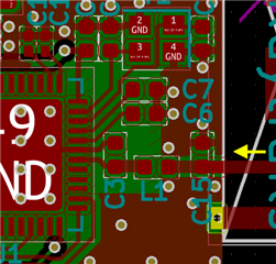
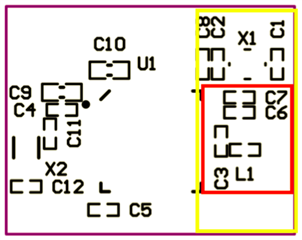
It's reasonable to avoid extra work recalculating the matching network and keep it intact. Also, replacing the 32MHz crystal (which itself is of the same footprint) capacitors won't really change anything:

But how about other elements? Would it be safe to follow WLCSP BOM as a packaging guideline?

Also, for my understanding moving them won't affect RF performance, right?

Thanks!

  • Hi Kaja!

    I've ensured my design is 1.6 mm PCB. Thank you!

    I'm on the KiCAD so tried to re-create reference design as accurately as possible, however as you and zigenz pointed out there may be too many factors impacting the performance. The device is in prototyping stage, but as it goes further I'm interesting in doing comprehensive RF analysis. I'll appreciate if you could point me to what exactly I need to do in order to get it there.

    To get an idea what I'm doing the board figures are at http://gerblook.org/pcb/hkSbzZuF7ddHB3mzygbcsZ (board size is 17mm x 28 mm).

    And here is a hi-res version of the radio path:

  • Hi Mike, 

    from what I can see on the layout, I see that you are missing capacitors on P0.25 and P0.26, due errata 138. You could also use the alternative workaround, grounding the pins. 

    It would be beneficial to be able to give you a full review, if you could upload schematic and the gerber files. 
    --> if you would like them to be private, create a new ticket, private ticket, and just reference this case. 


    Best regards,
    Kaja

  • Yeah, sure. Here it is:

    [files were removed]

  • Have you used the antenna before? 

    You might need at least one shunt component, to help with impedance matching of the antenna. 

    The rest looks fine! 

    To test RF performance, see: whitepaper.
    For antenna tuning, see: whitepaper.

    Let me know if you don't have the right equipment.

    Best regards,
    Kaja

  • Hi Kaja,

    thank you a lot for the review!

    No, I haven't used the antenna to the day. It's designed to match 50 Ohm at 2.45 GHz so I hoped to do adjustments using the provided pi network. The section 53.7 of the product specification v4 also suggests to use it for antenna tuning. But after reading the DevZone far and wide (BTW those whitepapers are simply brilliant!) I found it seems rather recommended to keep the network intact and use additional pi-network for chip-antenna or, just like you noticed, a shunt component for a PCB. Thus I've put C15 (0402) as follows:

    Hope that the board will have acceptable performance for prototyping, but it would be nice to fine tune it and my other device in the end. For the second device (which is counterpart to this one) I'm not so constrained in space so will be able to preserve another LC for antenna. Unfortunately, have no equipment for that.

    Okay, so answering the original quesiton:

    1. reproduce nRF52 matching network area as close as possible to the reference design; not only values, but element sizes, placement, and vias matter.
    2. the reference pi network is designed for FR4 of 1.6 mm thick, 1 oz/ft^2
    3. either for PCB or chip-antennas keep space for their own pi network
    4. ensure ground plane is covering the radio path, do not route anything over it
    5. antenna feed line should obviously match 50 Ohm
    6. check power lines and pins near the radio - they shouldn't be the noise source
    7. other components which are not located near radio pins are free to change and move

    P.S. Thanks again for pointing to the P0.25 & P0.26 issue! I've terminated them with 12pF capacitors (again, overlooked that due to the outdated spec).

Related