This post is older than 2 years and might not be relevant anymore
More Info: Consider searching for newer posts

Requirements for a PCB design review

Hi
Since we're almost done with the programming for our application we would like to move from the Development Kit to a custom board as similar as possible to the final PCB, the design is based on the reference design for the nRF-52810, although we're gonna produce only a few boards for testing, we would like to have some feedback from the experts in order to do modifications or fix what's wrong before manufacturing.

Which files do I need to provide to Nordic to request a review of my work?

Thanks in advance!

Parents Reply Children
  • Hi Diego,

    Diego Garcia said:
    The Antenna tunning Whitepaper says that I have to adjust the length of the antenna trace and add a shunt capacitor to match the impedance to 50 Ohms, and to achieve this, do I have to aquire an Vector Network Analyzer?

     - yes or you can send the pcb to me, and I can to the antenna tuning for you. 

    Diego Garcia said:
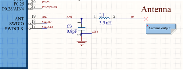
    Also, is the connection of the shunt components shown in the reference design?

     - No, this is because the reference design is for the chip, what matching components you need for the antenna is different, dependent on what type of antenna you choose. 

    Best regards,
    Kaja

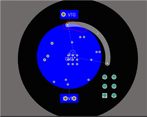
  • 1.-I pretend to use the PCB antenna from your nRF51822-Beacon since I was said that it was possible, so I copied the trace from the design files. Should I make the trace larger to ease the tunning?


    2.-That said, the shunt component should be placed right at the ANT pin or after the inductor?

    3.-Also, I've read that to measure current consumption with an oscilloscope, a low-value resistor should be placed in series with the power source (coin battery), but what is the proper place to put the resistor? Does it have to be after the battery retainer and before the chip?

Related