
hi, guys. I'm prepareing the Korea certification, KC, with nRF51822 BLE system. I'm progressing to get KC by certification agency. Today, They will have RF signal test and have to connect SMA cable on board, asked me let them know which components are matching circuit on board because they have to measure RF signal without matching circuit attached image is referance schematic on datasheet. I have some question about that.
-
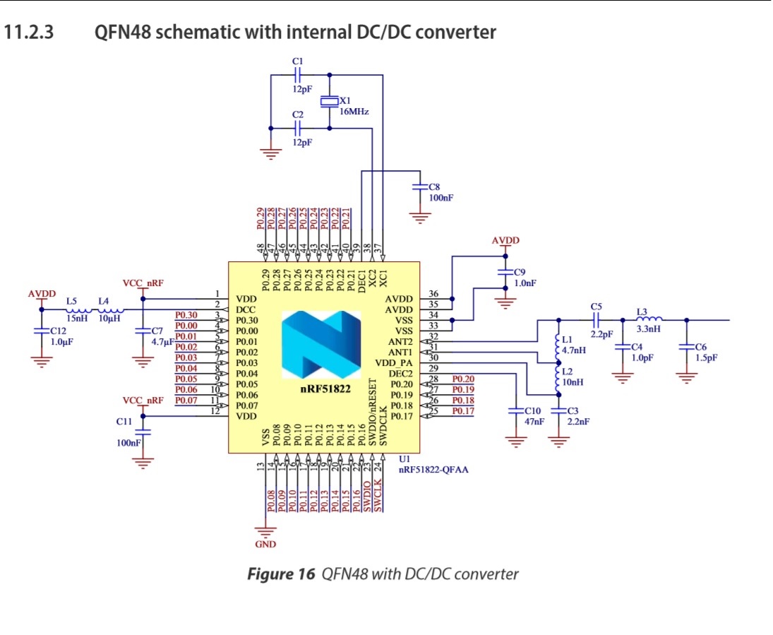
In the nRF51822 datasheet, all components(L1,L2,C3,C5,C4,L3,C6) after ANT1, ANT2, VDD_PA are matching circuit(like page.59). is it correct?
-
If I except matching circuit, the all components after ANT1, ANT2, VDD_PA should be removed?
2-1) If 2) is right, then which point i have to connect the SMA cable for measure RF signal, ANT1? or ANT2? if all component are removed and measure Rf signal on ANT1 or ANT2, the signal will be weak cos VDD_PA is not connect to ANT1/ANT2? if the signal too weak for that, may i keep the L2,C3 for VDD_PA to ANT2 and measure the signal on ANT2?
2-3) If 2) is wrong, which component will be keep on the board? maybe I'm wrong but I think L1, L2, C3 maybe keep the on board, becuase L1 is sum ANT1/ANT2, L2 is supply power for RF amp to ANT1/ANT2 from VDD_PA, C3 is decouple capacitor for VDD_PA. is it right? if L1/L2/C3 keep, remove C5 and connect the cable between L1 and C5, is it right?
Please, As soon as possible anybody let me know how to i should.
regard from korea. thx
