This post is older than 2 years and might not be relevant anymore
More Info: Consider searching for newer posts

programming custom NRF52840 soc with PCA10056 DK

Hi,

I bought a custom nrf52840 board and I need to program my firmware on this SOC with PCA10056 DK debug output port. in below you can see part of shematic of my custom board.
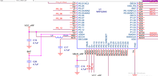
as you can see regulators are configured in High voltage mode where battery voltage(4.2v) is connected to VDDH and VDD voltage (expected to be 3.3v) is generated by the REG0. 

as I read in NORDIC froums by default REG0 is configured to generate 1.8V voltage and then soc work with 1.8v and could not be programmed with PCA10056 DK. 

so in order to program soc I want to disconnect battery from my board and then connect custom board to PCA10056 DK p20 port like below:

SWIO -> DK SWIO

SWCLOCK -> DK SWCLOCK

GND-> DK GND DETECT

VCC_nRF -> DK VDD_nRF

and also I think that I need to short SB47 as I need to supply voltage to my soc board from DK.

now, are above description correct?? this wouldn't damage to anything?? just because I have one board I do not want damage it.

thanks.

Parents
  • Hi,


    You should not damage anything, so programming devices in development should not be a problem. The REG0 regulator stage is not designed for being operated this way, and we have not verified the IC for use in this way, so we can not guarantee that it will stay shut of, and that it will not take damage. This means that for production programming at least you should not do this, but then you will probably use a programmer that supports 1.8 V anyway.  If you only have one board you might want to strap VDDH to VDD while programming just to be sure.


    Best regards,

    Andreas

  • Thanks for your response.

    after shorting SB47 jamper on PCA10056 DK, I Connected pins of my custom soc like below to P20 port of my PCA10056 DK:

    CustomSOC -> PCA10056 DK

    ------------------------------------------------------------

    SWDIO         -> SWDIO

    SWDCLK     ->  SWDCLK

    VBAT(means VDDH pin)      ->  VDDnRF

    VCC_nRF(means VDD pin) ->  VDDnRF'

    GND                                     ->  GND of PCA10056 board

    as VDDnRF and VDDnRF' has same output voltage, I assume that above configuration means that I straped VDDH to VDD. and also in P20 port I could not find any GND pin, so I connected it to GND pin of PCA10056 board.

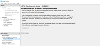
    I think that above configuration is correct but after connecting PCA10056 to PC nrfGo application did not recognize my custom soc and give below error.

    there is anything that I am doing wrong? and also power supply of custom soc is correct because I can see that after connection PCA10056 to usb, default app on custom soc work.

    thnaks

Reply
  • Thanks for your response.

    after shorting SB47 jamper on PCA10056 DK, I Connected pins of my custom soc like below to P20 port of my PCA10056 DK:

    CustomSOC -> PCA10056 DK

    ------------------------------------------------------------

    SWDIO         -> SWDIO

    SWDCLK     ->  SWDCLK

    VBAT(means VDDH pin)      ->  VDDnRF

    VCC_nRF(means VDD pin) ->  VDDnRF'

    GND                                     ->  GND of PCA10056 board

    as VDDnRF and VDDnRF' has same output voltage, I assume that above configuration means that I straped VDDH to VDD. and also in P20 port I could not find any GND pin, so I connected it to GND pin of PCA10056 board.

    I think that above configuration is correct but after connecting PCA10056 to PC nrfGo application did not recognize my custom soc and give below error.

    there is anything that I am doing wrong? and also power supply of custom soc is correct because I can see that after connection PCA10056 to usb, default app on custom soc work.

    thnaks

Children
Related