
Hi, I'm designing nRF52832 custom board, on 'single side' pcb.
To make VDD and GND lines connect, I used 4 jumpers, which have 0 ohms.
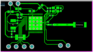
I designed with nRF52832-QFAB reference layout and pcb layout for internal LDO setup, but little difference from pcb layout to make on single side pcb.
But for some reason, I cannot use this pcb when I connect it to my DK board, using Keil. Everytime I connect and loading the example code on it, I got this error message.

I am absolutely have no idea what is the problem for this error, since with double side pcb with reference layout and pcb layout from this Nordic, there was no error like this.
Hope anyone can tell me what brings that kind of error. In my opinion, its because of soldering problem or the design problem, since same code is work for double side pcb.
Any recommends for the design or error will be very appreciated for me. Thank you.


