
Hi,
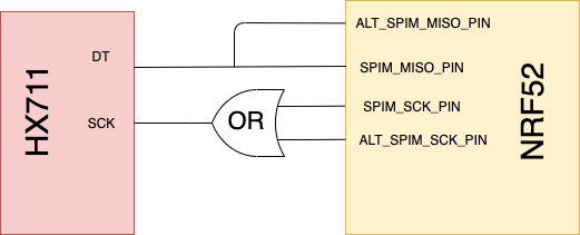
I have implemented a hx711 sensor readout with PPI, using SPIM and PWM peripherals. But for this is needed 4 GPIO and one external OR Gate. I wait for a LOW pulse on AL_SPIM_MISO_PIN, and Read SPI data and disable pulse detect. When SPI RX end, I put and extra pulse in ALT_SPIM_SCK_PIN (I only want Channel A with 128 Gain) and enable again pulse detect.
This is the code:
static void spi_init_hx711(void)
{
    nrfx_spim_xfer_desc_t xfer_desc = NRFX_SPIM_XFER_TRX(tx_buffer_spi, LS7366_SPI_BUFFER_SIZE, rx_buffer_spi, LS7366_SPI_BUFFER_SIZE);

    nrfx_spim_config_t spi_config = NRFX_SPIM_DEFAULT_CONFIG;
    spi_config.frequency      = NRF_SPIM_FREQ_500K;
    spi_config.ss_pin         = SPIM_SS_PIN;
    spi_config.miso_pin       = SPIM_MISO_PIN;
    spi_config.mosi_pin       = SPIM_MOSI_PIN;
    spi_config.sck_pin        = SPIM_SCK_PIN;
    ///spi_config.mode           = NRF_SPIM_MODE_1;
    spi_config.use_hw_ss      = true;
    spi_config.ss_active_high = false;


    ret_code_t err_code = nrfx_spim_init(&spi, &spi_config, spim_event_handler, NULL);
    APP_ERROR_CHECK(err_code);

}

void spim_event_handler(nrfx_spim_evt_t const * p_event,
                       void *                   p_context)
{

    if(p_event->type == NRFX_SPIM_EVENT_DONE)
    {
        NRF_LOG_DEBUG("TxDone\n");
        NRF_LOG_HEXDUMP_INFO(rx_buffer_spi,LS7366_SPI_BUFFER_SIZE);
        spi_tx_done = true;
    }
    else
    {
        NRF_LOG_DEBUG("Wrong Event\n");
        // Something is wrong
    }

}


static void hx711_spi_sampling_event_config()
{
    ret_code_t err_code;

    err_code = nrf_drv_ppi_init();
    APP_ERROR_CHECK(err_code);

    uint32_t spi_evt_addr;
    uint32_t spi_task_addr;
    uint32_t data_in_evt_addr;
    uint32_t put_clk_pulses_task_addr;
    uint32_t disable_ppi_channel_start_task_addr;
    uint32_t enable_ppi_channel_group_task_addr;


    err_code = nrfx_ppi_channel_alloc(&m_ppi_channel_detect_hx711_start_tx); //Detect TX Ready
    APP_ERROR_CHECK(err_code);

    err_code = nrfx_ppi_channel_alloc(&m_ppi_channel_stop_spi);
    APP_ERROR_CHECK(err_code);

    err_code = nrfx_ppi_group_alloc(&m_ppi_group_hx711);
    APP_ERROR_CHECK(err_code);

    err_code = nrfx_ppi_channel_include_in_group(m_ppi_channel_detect_hx711_start_tx, NRF_PPI_CHANNEL_GROUP0);
    APP_ERROR_CHECK(err_code);

    data_in_evt_addr = nrfx_gpiote_in_event_addr_get(ALT_SPIM_MISO_PIN); //DATAIN going low detect

    static uint16_t seq_values[] ={0};

    nrf_pwm_sequence_t const seq =
    {
        .values.p_common = seq_values,
        .length          = NRF_PWM_VALUES_LENGTH(seq_values),
        .repeats         = 1,
        .end_delay       = 0
    };

    spi_task_addr = nrfx_spim_start_task_get(&spi); //SPI START task address
    put_clk_pulses_task_addr = nrfx_pwm_simple_playback(&m_pwm1, &seq, 1,
            NRFX_PWM_FLAG_STOP |
            NRFX_PWM_FLAG_START_VIA_TASK);
    disable_ppi_channel_start_task_addr = nrfx_ppi_task_addr_get(NRF_PPI_TASK_CHG0_DIS);

    //1ST PPI CHANNEL
    err_code = nrfx_ppi_channel_assign(m_ppi_channel_detect_hx711_start_tx,
                                       data_in_evt_addr,
                                       spi_task_addr); //Start SPI RX
    APP_ERROR_CHECK(err_code);
    err_code = nrfx_ppi_channel_fork_assign(m_ppi_channel_detect_hx711_start_tx,
                                            disable_ppi_channel_start_task_addr); //Disable DIN Detect
    APP_ERROR_CHECK(err_code);


    //2ND PPI CHANNEL
    spi_evt_addr = nrfx_spim_end_event_get(&spi);
    enable_ppi_channel_group_task_addr = nrfx_ppi_task_addr_get(NRF_PPI_TASK_CHG0_EN);
    err_code = nrfx_ppi_channel_assign(m_ppi_channel_stop_spi,
                                      spi_evt_addr,
                                      put_clk_pulses_task_addr); //Put Extra pulses

    APP_ERROR_CHECK(err_code);
    err_code = nrfx_ppi_channel_fork_assign(m_ppi_channel_stop_spi, enable_ppi_channel_group_task_addr); //Renable MISO go down detection
    APP_ERROR_CHECK(err_code);

}

static void hx711_spi_init()
{

    ret_code_t err_code = nrfx_ppi_channel_enable(m_ppi_channel_detect_hx711_start_tx);
    APP_ERROR_CHECK(err_code);

    err_code = nrfx_ppi_group_enable(m_ppi_group_hx711);
    APP_ERROR_CHECK(err_code);

    err_code = nrfx_ppi_channel_enable(m_ppi_channel_stop_spi);
    APP_ERROR_CHECK(err_code);

    nrfx_gpiote_in_event_enable(ALT_SPIM_MISO_PIN, true);

}

static void pwm_init()
{
    uint32_t err_code;
// Config the pwm to set additional pulses in SPI
    nrfx_pwm_config_t const config1 =
    {
        .output_pins =
        {
            ALT_SPIM_SCK_PIN,                                       // channel 0
            NRFX_PWM_PIN_NOT_USED,                                        // channel 1
            NRFX_PWM_PIN_NOT_USED,                                        // channel 2
            NRFX_PWM_PIN_NOT_USED,                                        // channel 3
        },
        .irq_priority = APP_IRQ_PRIORITY_HIGH,
        .base_clock   = NRF_PWM_CLK_2MHz,
        .count_mode   = NRF_PWM_MODE_UP,
        .top_value    = 1,
        .load_mode    = NRF_PWM_LOAD_COMMON,
        .step_mode    = NRF_PWM_STEP_AUTO
    };
    err_code = nrfx_pwm_init(&m_pwm1, &config1, NULL);

}

static void spi_prepare_transfer(void)
{
    tx_buffer_spi[0] = 0xAA; //Dont worry about this number
    memset(rx_buffer_spi,0,3);
    nrfx_spim_xfer_desc_t xfer = NRFX_SPIM_XFER_TRX(tx_buffer_spi, 1, rx_buffer_spi, 3);
    uint32_t flags = NRFX_SPIM_FLAG_HOLD_XFER | NRFX_SPIM_FLAG_REPEATED_XFER | NRFX_SPIM_FLAG_NO_XFER_EVT_HANDLER;
    nrfx_spim_xfer(&spi, &xfer, flags);

}

int main(void)
{
    (...)

    spi_init_hx711();

    pwm_init();

    hx711_spi_sampling_event_config();

    hx711_spi_init();

    (...)


}
How can i delete the OR Gate, or extra PINs?
Thank you.

