This post is older than 2 years and might not be relevant anymore
More Info: Consider searching for newer posts

Custom nrf52832 board

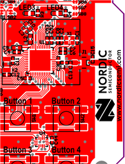
I want to create a small bluetooth device with the nrf52823 chip. I want to use a lithium battery cell to power the whole circuit and therefore it neet to be low power. On the chip, there are two inputs: one button and the battery voltage detector. There is also a buzzer connected to the chip via a 28v boost circut. I created a schematic with easyeda, but I dont kow if I designed it propertly. Here are my questions:

- does the circuit look right?

- did I pick the right parts?

- am I able to programm the custom board via the DCLK and  SWDIO pins through the nrf52 dk?

- does the battery need a seperate protection circuit?

- how do I design the nrf and ble antenna?

 Schematic_Beep Wallet_V3.2_20191120173356.pdf

BOM_Beep Wallet_20191120173443.csv

Thank you in advice

Jonas

Parents
  • I updated my circuit the second time.

    This time I tried to copy the nrf circuit from the Development Kit (parts are also mostly the same). The only big different here, is the the 32.768 Mhz cristal. The Load Capacitance is 6pf not 9pf (dk). Is that a problem ?

    Moreover I designed the ble antenna based on the documentations, but my pcb is only 0.6 - 0.8mm height instead of 1.6mm do I have to worry about that?

    I copied the NFC antenna from the development kit.

    I also added a battery discharge and overcharge protection.

    What do you think about the pcb ?

    v3_3.zip

    Jonas

  • Hi Jonas,

    I can't see the routing in your schematic, could you upload the schematic with routing?
    You can upload the altium file, if you have done the schematic there as well. 

    For the layout:
    1. Your missing ground plane in top and bottom layer, make solid and large ground planes. This will ensure proper grounding of the center pad, the components, and the antenna efficiency gets better the larger ground planes it sees. 
    2. Start with the reference designs, the altium files so that you get a good start point for where the components should be places and the ground planes around. 
    3. The antenna should be placed on the edge of the board, then rotate the chip so that you get the ANT pin facing the antenna:


    4. The trace from the radio matching network to the antenna, should be a 50 Ohm transmission line. The calculation of the transmission line will have to be calculated based on the substrate and distance to ground:

    In the bottom layer under the transmission line there should be solid ground. 

    Feel free to upload updated files, when they are ready. 

    Best regards,
    Kaja

Reply
  • Hi Jonas,

    I can't see the routing in your schematic, could you upload the schematic with routing?
    You can upload the altium file, if you have done the schematic there as well. 

    For the layout:
    1. Your missing ground plane in top and bottom layer, make solid and large ground planes. This will ensure proper grounding of the center pad, the components, and the antenna efficiency gets better the larger ground planes it sees. 
    2. Start with the reference designs, the altium files so that you get a good start point for where the components should be places and the ground planes around. 
    3. The antenna should be placed on the edge of the board, then rotate the chip so that you get the ANT pin facing the antenna:


    4. The trace from the radio matching network to the antenna, should be a 50 Ohm transmission line. The calculation of the transmission line will have to be calculated based on the substrate and distance to ground:

    In the bottom layer under the transmission line there should be solid ground. 

    Feel free to upload updated files, when they are ready. 

    Best regards,
    Kaja

Children
No Data
Related