
Hi!
I'm having trouble getting any response from an NRF52840 MCU on a custom board we've made.
I'm hoping someone will be able to point me in the right direction by detailing how they would go about debugging the problem here.
I'm using:
1. Jlink plus debugger with SWD connections connected to the SWD IOs on my board. I use SWDCLK, SWDIO, Vin (Either VDD or VDDH as specified in the NRF datasheet) and GND.
2. Jlink Connect to define the SWD parameters (Set to SWD, which device I use, connection speed etc)
3. My custom PCB was designed based on one of the reference circuits, so I think the design is solid in so far as it follows the reference.
What I get:
1. The Jlink attempts to form an SWD connection, but is unable to.
2. I measure good working voltage over the VDD and VDDH lines.
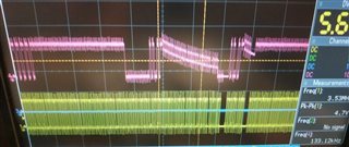
3. I looked at the SWD IO and CLK lines using a scope, and I get what I expect to see. The clock is solid and the initial startup sequence is sent over the IO line (50 clocks high IO, then 0x79E7 msb first etc). I do get 'strange' behavior on the IO line on what look to me to be the parts where the debugger is waiting for the target to respond. It looks as though the debugger has placed the IO line on high Z on its end, and now the voltage is discharging naturally similar to how it would in an RC circuit. I will note that when measuring the same line with the custom board completely disconnected (meaning the IO and CLK lines are not connected to anything besides the scope) I see the same 'strange' behavior. This means that my board behaves the same way as 'nothing' behaves when connected to the debugger. Not a good sign. See the image attached.
So far I've tried:
1. Connecting the debugger to an MCU on one of my DKs, using the same SWD lines. This passed successfully, so I know I'm working with the debugger properly using SWD.
2. I've tried several custom boards in the hopes there was some flaw with a few of them. All of them fail the same way.
3. lowering the connection speed as specified in this segger debugging manual
4. Trying to set the boards to normal and high power modes (Vin via VDDH and VDD pins or VDDH only with higher voltage) as per the Nordic specifications).
5. Extensively looking online and in forums for advice.
What I'm looking for:
1. Any advice as to how to proceed.
2. Any advice as to how to measure the 32MHz oscillator while its on board, or while its off board
3. Any other questions on points which seem relevant to test
Thanks in advance!

