This post is older than 2 years and might not be relevant anymore
More Info: Consider searching for newer posts

How critical are polygon cutouts under component pads in RF nets in nRF9160 DK design.

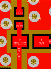
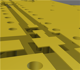
I understand the reason for the polygon cutouts under component pads in the RF nets in nRF9160 DK design (and others). However, at LTE and GPS frequencies this doesn't seem as necessary. I'm curious, whether you (Nordic) do this as best practice or whether you started doing this due to some actual hardware issues during testing/certification on a previous design without the polygon cutouts.

I am trying to understand how critical these might be for LTE and GPS nets in my design and how likely it's to negatively affect it's  performance and chances of passing certification if I omit them..

Thank you!

Parents
  • The cutouts under the component pads are there to reduce parasitic capacitance to ground. For single frequency antennas, like the GPS antenna and if the LTE modem is used on only one band, this is less important.

    If you plan to use several frequency bands, I'd recommend to have the cutouts as it makes tuning the LTE antenna for a higher bandwidth somewhat easier. This can also be a case for certification as it's usually a requirement to have a  minimum radiated output power. 

Reply
  • The cutouts under the component pads are there to reduce parasitic capacitance to ground. For single frequency antennas, like the GPS antenna and if the LTE modem is used on only one band, this is less important.

    If you plan to use several frequency bands, I'd recommend to have the cutouts as it makes tuning the LTE antenna for a higher bandwidth somewhat easier. This can also be a case for certification as it's usually a requirement to have a  minimum radiated output power. 

Children
Related