This post is older than 2 years and might not be relevant anymore
More Info: Consider searching for newer posts

nRF5340 Antenna/Inductor Layout

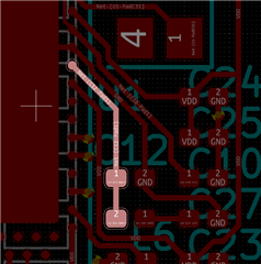
The recommended circuit in the v0.5 nRF5340 product spec differs a little from the nRF5340-PDK and I'm trying to understand the minimum requirements for an antenna. The spec shows the antenna (L6) as a 0201 sized, 2.2nH high-frequency inductor—is this all that is needed to do short-range TX/RX? For example, a TDK MHQ0603P2N2BT000?

My board has L6 off of pin L31 (image bottom) with C12 (image middle) grounded through J31 to the chip pad, per the spec. We aren't looking for awesome wireless performance, but it's unclear if this inductor is meant to stand alone, or requires a trace antenna on the other end?

Parents
  • Hi,


    L6 is not the antenna, it is just an inductor in the matching network. It is added to suppress the harmonics generated by the radio PA, as without it (or with a non-optimal value) the radio might transmit more harmonics('unwanted emissions') than allowed by regulatory bodies. The radio will generate and transmit the fundamental signal whether it is there as a 2.2nH or a 0 Ohm. The part you referenced is most likely fine, but you should for sure test it before applying for certification testing, if you plan on doing that. This might also change in upcoming revisions of the IC/ref design.


    Looking at the DK design:

    • Yellow: antenna, trasforming a radiated field to/from the radio transmission line.
    • Green: antenna tuning capacitor, tuning the antenna to 50 ohm for maximum power transfer.
    • Blue: coaxial switch connector, for hooking on a coaxial probe cable for e.g. RF power and harmonics measurements.
    • Brown: antenna matching network, matching the radio to 50 ohm.


    It seems that you in your layout have not replicated the reference layout. This is just as important, if not more, than the reference schematic if you want good RF performance. Also not sure I understand if you have an antenna or not, in any case this must be placed along the edge of the board and have a keepout to metal/ground like shown above. The reason there is not an antenna in the PS reference design is that one might connect a switch, filter, coupler, front-end module or other RF system component here, instead of an antenna.


    Best regards,

    Andreas

Reply
  • Hi,


    L6 is not the antenna, it is just an inductor in the matching network. It is added to suppress the harmonics generated by the radio PA, as without it (or with a non-optimal value) the radio might transmit more harmonics('unwanted emissions') than allowed by regulatory bodies. The radio will generate and transmit the fundamental signal whether it is there as a 2.2nH or a 0 Ohm. The part you referenced is most likely fine, but you should for sure test it before applying for certification testing, if you plan on doing that. This might also change in upcoming revisions of the IC/ref design.


    Looking at the DK design:

    • Yellow: antenna, trasforming a radiated field to/from the radio transmission line.
    • Green: antenna tuning capacitor, tuning the antenna to 50 ohm for maximum power transfer.
    • Blue: coaxial switch connector, for hooking on a coaxial probe cable for e.g. RF power and harmonics measurements.
    • Brown: antenna matching network, matching the radio to 50 ohm.


    It seems that you in your layout have not replicated the reference layout. This is just as important, if not more, than the reference schematic if you want good RF performance. Also not sure I understand if you have an antenna or not, in any case this must be placed along the edge of the board and have a keepout to metal/ground like shown above. The reason there is not an antenna in the PS reference design is that one might connect a switch, filter, coupler, front-end module or other RF system component here, instead of an antenna.


    Best regards,

    Andreas

Children
No Data
Related