
I have worked with the nRF24L01+ for a couple of days now without getting it to work. The setup of the chip is done as described below, without any luck of getting a communication going from one chip to another. The routines are tested on a board with a TM4C123G micro controller with two nRF24L01+ breakout boards mounted to two separate SPI channels. The SPI communication seems to work fine (checked with a scope).
No matter what data is sent, the received data is all zeros. The status register does not change on either of the nRF24L01+ chips and seems to be the same before and after a send/receive.
Hopefully some of you can verify that the routines below is correct or point out the mistakes. Any help is appreciated.
Thanks in advance :-)
Read/Write routine
- Wait 10 µs
- Set CS low (chip select)
- SPI put (W_REGISTER + register address)
- SPI get STATUS byte
- For all data bytes
- If read mode: SPI put NOP and save returned value from SPI get
- If write mode: SPI put data byte and discard returned value from SPI get
- Wait 10 µs (for each byte)
- Set CS high (chip deselect)
Initialization
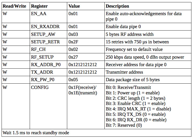
With the Read/Write routine shown above, the following operations are done in order to initialize the device (after voltage is applied to the MCU and nRF24L01+):
Reset
- Set CS low (select chip)
- Wait 10 µs
- SPI Put 0x27 (W_REGISTER + STATUS)
- Read 1 byte with SPI (discarded STATUS byte)
- Wait 10 µs
- SPI Put 0x70 (Clear IRQ bits in STATUS)
- Read 1 byte with SPI (discarded STATUS byte)
- Wait 10 µs
- Set CS high (deselect chip)
Transmit
- Send FLUSH_TX command
- Send W_TX_PAYLOAD with 5 byte data
- Wait 10 µs
- Set CE high (chip enable)
- Wait 20 µs
- Set CE low (chip disable)
- Wait 10 µs
Receive
- Set CE high (chip enable)
- Wait 130 µs
- Send command R_RX_PAYLOAD and save 5 bytes of data
- Reset registers (with routine above)
- Wait 130 µs
- Set CE low (chip disable)
