Hi everyone,
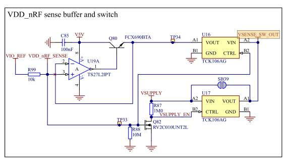
I am looking the schematic of nRF52840 (PCA10056) and I am a bit confused with the Power Sources (sheet 7 of 7).
There are three load switches that prioritize the power sources. What I understand so far is that when the 5V boost converter is ON then LiPo battery and ext. source are ignored and when ext. source is detected LiPo battery is ignored.
But I cannot understand the schematic. I mean, VSUPPLY line is connected on the input of each load switch.. It shouldn't be connected to the switches' output to get the voltage of the corresponding source (VREG, VBAT, VEXT)?
Also on the schematic, there is the VDD signal. I cannot figure out where is coming from...
1. Where is coming from the VDD signal based on the schematic?
2. VDD value depends on the power source (VDD, VBAT, VEXT)?
Thanks in advance!!