This post is older than 2 years and might not be relevant anymore
More Info: Consider searching for newer posts

Analyzing automatic current switch

I'm trying to learn more about automatic current range switch and stumbled across Nordic's nRF6707 power profiler kit that has very interesting topology to choose between three different current ranges.

Now I "understand how" this circuit works but what I'm having hard time with is figuring out how to start analyzing thresholds, different start conditions and in general doing deeper analysis of this circuit in order to have proper understanding of how it works.

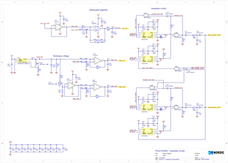
Here is the screenshot of the schematic portion for automatic switch:

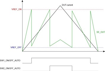
What I'm having trouble with and could really use help with, is suggestions on how to start analyzing automatic switch portion. I'm not sure how to find steady-state values and also initial conditions (although I assume both SW1 and SW2 should be off on power-up with no load) and also how to analyze transitions when measured current crosses Vref On/Off thresholds (in up or down direction).

Any help or suggestions would be much appreciated!

Parents
  • I've got a reply from our designer:
     

    The top circuit on the left-hand side is just a differential to single-ended amplification of the measured current, with some low pass filtering to “slow down” the signal. On the bottom left you will find a circuit to set reference voltages for “turn on” and “turn off” the different stages. The reference voltages are set in a way that it matched the amplification of the signal and that it triggers switching before the ADC saturates. What is important on the left-hand side is that when a switch is triggered, “SE_OUT” hits “VREF_ON”, the “SE_OUT” will also drop, so the “VREF_OFF” must be lower than this to avoid oscillations. The difference between “SE_OUT” just after a switch and “VREF_OFF” defines the hysteresis of the switching.


    On the right-hand side resides the logic that decides which range that should be used. Without thinking so much about the absolute levels, the easiest way to understand the logic is to imagine that the current consumption of your DUT is a triangle pulse. The “SWx_ON/OFF_AUTO” result of a triangle pulse like that will be like the figure below. The analysis of all the logic levels between the comparators (U11-U14) and “SWx_ON/OFF_AUTO” I think you will understand best if you try to have a look at yourself. One key thing is the use of the “SHDN” pin of the comparators. This is used in a way that only the comparator(s) that “have work to do” in the current state is enabled. When the comparator is in SHDN mode, Q is Hi-Z.


    Using the triangle pulse as an example:

    • Starting from 0, only U11 is enabled
      • U11 is ready to enable switch 1 if the current should increase
    • When “SE_OUT” hits “VREF_ON” U11 triggers and sets SW1_ON/OFF_AUTO = 1 as well as disables U11 and enables U12 and U13.
      • U12 is ready to disable switch 1 if the current should decrease
      • U13 is ready to enable switch 2 if the current should increase
    • When “SE_OUT” hits “VREF_ON” again U13 triggers and sets SW2_ON/OFF_AUTO = 1 as well as disables U12 and U13 and enables U14.
      • U14 is ready to disable switch 2 if the current should decrease


    When the signal is falling this will be in reverse order, with comparators turning off at “VREF_OFF”.


    The resistors R39, R42, R43, and R46 keeps the correct signal level when comparators are in SHDN mode, the buffers and RC at the end are used to "slow down" the signal to avoid oscillations.

Reply
  • I've got a reply from our designer:
     

    The top circuit on the left-hand side is just a differential to single-ended amplification of the measured current, with some low pass filtering to “slow down” the signal. On the bottom left you will find a circuit to set reference voltages for “turn on” and “turn off” the different stages. The reference voltages are set in a way that it matched the amplification of the signal and that it triggers switching before the ADC saturates. What is important on the left-hand side is that when a switch is triggered, “SE_OUT” hits “VREF_ON”, the “SE_OUT” will also drop, so the “VREF_OFF” must be lower than this to avoid oscillations. The difference between “SE_OUT” just after a switch and “VREF_OFF” defines the hysteresis of the switching.


    On the right-hand side resides the logic that decides which range that should be used. Without thinking so much about the absolute levels, the easiest way to understand the logic is to imagine that the current consumption of your DUT is a triangle pulse. The “SWx_ON/OFF_AUTO” result of a triangle pulse like that will be like the figure below. The analysis of all the logic levels between the comparators (U11-U14) and “SWx_ON/OFF_AUTO” I think you will understand best if you try to have a look at yourself. One key thing is the use of the “SHDN” pin of the comparators. This is used in a way that only the comparator(s) that “have work to do” in the current state is enabled. When the comparator is in SHDN mode, Q is Hi-Z.


    Using the triangle pulse as an example:

    • Starting from 0, only U11 is enabled
      • U11 is ready to enable switch 1 if the current should increase
    • When “SE_OUT” hits “VREF_ON” U11 triggers and sets SW1_ON/OFF_AUTO = 1 as well as disables U11 and enables U12 and U13.
      • U12 is ready to disable switch 1 if the current should decrease
      • U13 is ready to enable switch 2 if the current should increase
    • When “SE_OUT” hits “VREF_ON” again U13 triggers and sets SW2_ON/OFF_AUTO = 1 as well as disables U12 and U13 and enables U14.
      • U14 is ready to disable switch 2 if the current should decrease


    When the signal is falling this will be in reverse order, with comparators turning off at “VREF_OFF”.


    The resistors R39, R42, R43, and R46 keeps the correct signal level when comparators are in SHDN mode, the buffers and RC at the end are used to "slow down" the signal to avoid oscillations.

Children
No Data
Related