This post is older than 2 years and might not be relevant anymore
More Info: Consider searching for newer posts

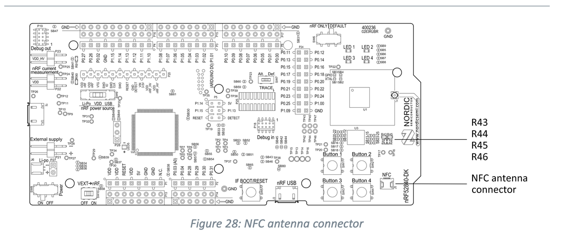
[nRF52840 DK dev board] Debug In (P18) Out (P19) pinout - DYI cable

Hi there,

Because of the current corona virus I could order a debug in/out cable for the Segger's build-in debugger (P18 & P19). But I have the cable it self and slot compatible sockets.
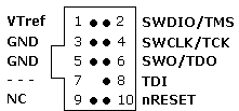
What I need is the pinout to made the whole debug cable by myself.

Is this the 10-pinout layout for both P18 & P19?
Parents
  • Hi Redshifter, 

    I'm not sure what you are planning to do.  But I assume you know that you can get the hardware design (schematic and layout) of the nRF52 boards from our website. 
    P18 and P19 follow exactly the pins showed in your image. 
    You need at least 4 pins, Vtref, GND, SWDIO, and SWCLK. Pin 9 is connected to 3 and 5 to work as Ground detect. It's then routed to the Segger OB chip to detect if there is a board connected to the debug out/in port. 

Reply
  • Hi Redshifter, 

    I'm not sure what you are planning to do.  But I assume you know that you can get the hardware design (schematic and layout) of the nRF52 boards from our website. 
    P18 and P19 follow exactly the pins showed in your image. 
    You need at least 4 pins, Vtref, GND, SWDIO, and SWCLK. Pin 9 is connected to 3 and 5 to work as Ground detect. It's then routed to the Segger OB chip to detect if there is a board connected to the debug out/in port. 

Children
No Data
Related