This post is older than 2 years and might not be relevant anymore
More Info: Consider searching for newer posts

Could deviations from nRF52832 reference design cause chip to die during DTM testing?

We recently ported to the nRF52832 and our electrical engineer had to make a couple changes from the reference design due to space constraints. The port has worked well during internal testing but unfortunately a unit running the standard DTM firmware died on the company that is testing it for CE Marking. The testing company is using nRFgo Studio with our unit being powered by UART and a lipo battery. They said it worked correctly for one day of testing and then the next day it wouldn't power up.

We have since run a lot of tests internally on multiple units with the DTM firmware controlled by nRFgo Studio and unfortunately have not been able to recreate the issue. The testing company thinks the issue could be caused by our deviation from the reference design, specifically the changes on the capacitors on VDD. 

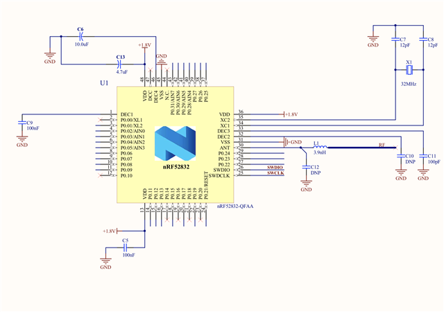
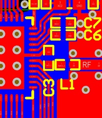
I've included our schematic and layout below. Could our minor deviations from the reference design cause the nRF to die during DTM testing? What (if any) issues would you expect these changes from the reference design to cause? Please let me know if any additional information will help. Thanks for any input!

  • Hello Wes,

    Can you clarify this please?  " Unit being powered by UART and a lipo battery."  Do you have a external LDO or DC/DC supplying the 1.8vdc?

  • Hi Jay,

    Our board is usually powered by a 3V CR2450 coin cell battery through a 1.8v LDO to the VDD pins. We also have a port for testing that directly exposes pins that the UART plugs into and puts 3.3V directly on the VDD pins. When they were running the DTM testing they had the battery connected and the UART plugged in so VDD was receiving 1.8V from the battery/LDO and 3.3V from the UART. Does that make sense? Thank you for any help.

  • Please review the Datasheet as it relates to max voltage on the GPIO in relation to the VDD.  Section 20.4.1 page 154.   The UART at 3.3V with VDD at 1.8V is not ok.  I believe this is why the  part stopped working.  On a separate somewhat unrelated note,  the RF output Matching / harmonic  network is incorrect.  C12 should be populated. The trace from C12  to the VSS_PA is to long and will effect harmonic content.   The design is also missing a matching network for the Antenna.   There should be no traces or components near the antenna. 

  • The deviations from the reference layout is so large that there is a high probability that it will fail CE testing due to spurious emissions.

    The matching network shall look like this, note like C3 here is grounded: 

    Use a top side ground plane and make sure you don't route ground with tracks, but connect grounded pis to the ground plane. Use plenty of vias between the two ground planes. 

    Study the reference layout and make sure you copy it as best as you can. The center pad shall be grounded with at least 16 vias to the bottom side ground plane. 

  • Jay, thanks so much for reviewing our circuit. That makes sense about the UART at 3.3V and it sounds like that is probably what broke the part. We originally had C12 populated and were having signal strength issues. When we removed C12 the signal strength improved quite a bit and our engineer considered it a basic form of network matching. Would the items you pointed out only cause signal strength/efficiency issues or could it cause issues with chip functionality and/or other issues?

Related