
Hello,
I'm developing a coin-sized board based on the nRF52840 and the nRF52833 in aQFN73 package. The PCB has only two layers with the bottom layer dedicated to ground plane with CR2032 battery attached directly to it. For this reason the board has no routing beneath the chip, and there are no internal layers.
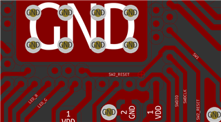
The stackup is nearly good, but the device do miss the reset pin. The AC13 pin is located on an inner row and route it out of its location is tricky. In attempt to address it somehow I've drooped number of inner pins and guided the track (SW2_RESET on the picture) like this:
Need your expert advice, is this idea any good? If not, what might be a better option?
Thanks!
-- Mishka

