Hi there,
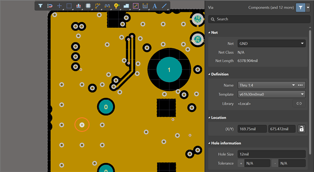
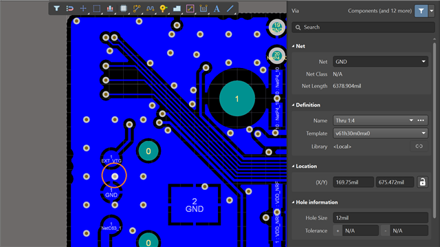
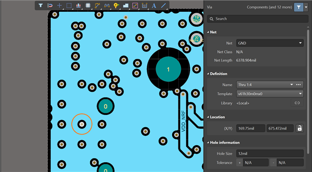
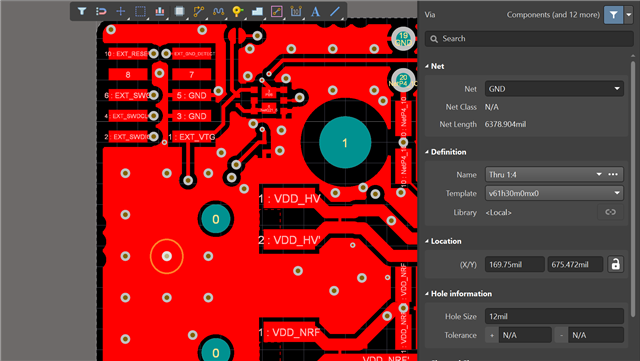
I have a few questions regarding the Development Kit hardware design. I just bought up the polygon pour manager. I noticed that all layers except Mid-Layer 2 are netted to GND. What does ‘VDD_SAM’ allude to in the Mid-Layer 2 polygon pour net? What voltage level does ‘VDD’ refer to in the other Mid-Layer 2 polygon pour net? I have attached images of the Top and Mid-Layer 2 polygon pours:
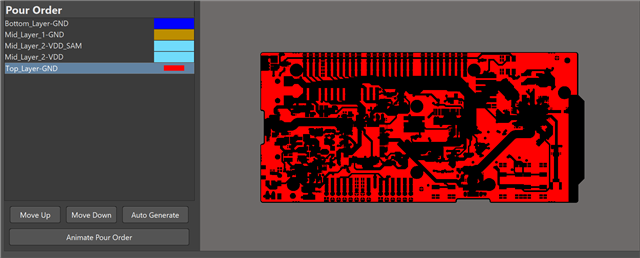
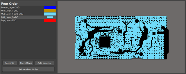

I see that 'VDD_SAM' is only poured over the area of the interface chip.
I’ve also noticed that there are vias placed all throughout the board, attaching all the ground planes together. Is this advisable in a custom design with four layers? If so, what is the common practice around this (i.e. distance between GND vias)? I have selected one via (circled in orange), and cycled through the layers. Notice the lack of connection between the via and the pour and Mid-Layer 2. I’m assuming this is because the vias are just connecting the ground pours?