This post is older than 2 years and might not be relevant anymore
More Info: Consider searching for newer posts

nRF24LU1 PCB Layout files

Hello,

I am evaluating different printed antenna options for my Nordic design using nRF52 series ICs.  The small size of the meandered antenna used in the nRF24LU1 USB dongle seems like a possible contender.

Q1.  Can you provide the PCB layout files for the nRF24LU1 design?  The Altium files would be very helpful if not gerber data.


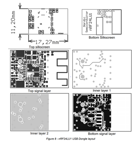
Q2.  For this antenna, where or what is the formula that calculates PCB trace width/thickness for a given board thickness?  For example, what should my trace width and thickness be if I use a 0.031" thick board?

Thank you,

E

Parents Reply Children
  • Hello,

    1.  Thank you for the link.  I was able to find the files I needed.

    2.  Sorry but this does not help me much.  Saying that it is not easily calculated is the equivalent of saying look for it on the internet.  I don't need any help tuning the antenna, I just want to understand how to go about determining trace width and thickness.  I could use a simple online calculator for this.

    Best Regards,

    E

  • Hi,


    2. If you mean the transmission line width and gap then yes, you can use a simple calculator, we often use AppCAD for this. If you mean the antenna trace width then no this can still not be calculated easily, the meandering pattern is optimizded for this antenna trace width, by changing it you risk degrading the performance.


    Best regards,

    Andreas

Related