Hi there,
I am in the process of developing a custom PCB using the nRF52833 SoC. This board is quite simple, and doesn't use many of the pins of the nRF52833 SoC.
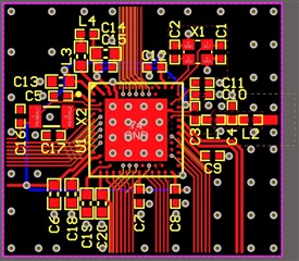
I am using reference layout 4 from Nordic. Within the associated documentation, it is strongly recommended not to change the reference layout to ensure optimal performance. Thus I have a few questions:
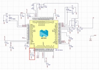
- Due to the fact that I am using very few pins on the nRF SoC, I have deleted many of the superfluous traces, effectively leaving the pins NC. Is this fine?
- I have refrained from putting any USB infrastructure on the board. This means I have no use for VBUS and the associated capacitor (C20), is it fine to delete C20 (and the trace) from the reference layout? I have attached screenshots of my schematic (with C20 highlighted in red) and the original Var 4 reference layout PCB.
Another question which is unrelated: What type of antenna would you advise for good performance in cross-polarisation and co-polarisation scenarios? I am currently using a trace antenna (similar to the antenna on the nRF52833 DK). But I'm wondering if a meander or chip antenna might be more effective. What are your recommendations? I assume RF testing has been performed on the nRF52833 DK antenna with different polarisation settings?
Cheers